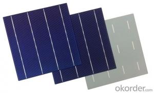
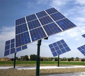
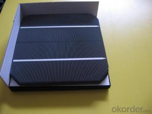
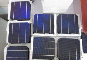
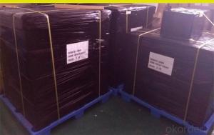
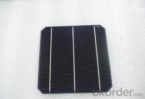
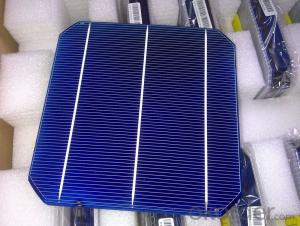
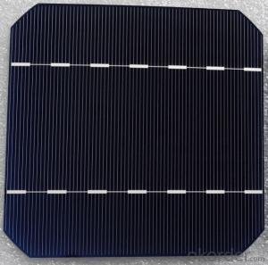
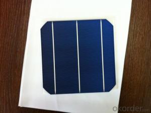
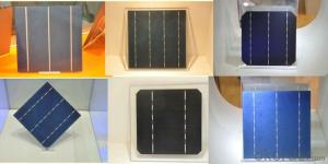
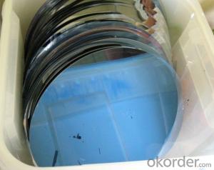
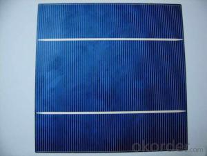
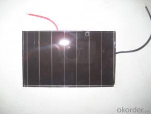
Silicon Wafer Solar Cell Panels - High Quality A Grade Mono Crystalline 5V 18.4% Solar Cells
- Loading Port:
- Shanghai
- Payment Terms:
- TT OR LC
- Min Order Qty:
- 1000 pc
- Supply Capability:
- 100000 pc/month
OKorder Service Pledge
OKorder Financial Service
You Might Also Like
Specifications
hot sale solar cell
1.16.8%~18.25% high efficiency
2.100% checked quality
3.ISO9001/ISO14001/TUV/CE/UL
4.stable performance
We can offer you the best quality products and services, don't miss !
POLY6'(156*156)
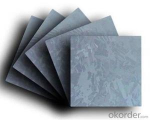
Polycrystalline Silicon Solar cell
Physical Characteristics
Dimension: 156mm×156mm±0.5mm
Diagonal: 220mm±0.5mm
Thickness(Si): 200±20 μm
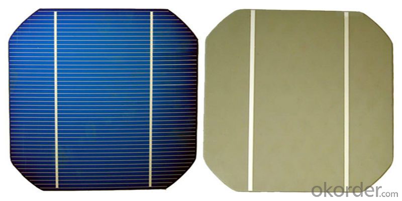
Front(-) Back(+)
Blue anti-reflecting coating (silicon nitride); Aluminum back surface field;
1.5mm wide bus bars; 2.0mm wide soldering pads;
Distance between bus bars: 51mm . Distance between bus bars :51mm .
Electrical Characteristics
Efficiency(%) | 18.00 | 17.80 | 17.60 | 17.40 | 17.20 | 16.80 | 16.60 | 16.40 | 16.20 | 16.00 | 15.80 | 15.60 |
Pmpp(W) | 4.33 | 4.29 | 4.24 | 4.19 | 4.14 | 4.09 | 4.04 | 3.99 | 3.94 | 3.90 | 3.86 | 3.82 |
Umpp(V) | 0.530 | 0.527 | 0.524 | 0.521 | 0.518 | 0.516 | 0.514 | 0.511 | 0.509 | 0.506 | 0.503 | 0.501 |
Impp(A) | 8.159 | 8.126 | 8.081 | 8.035 | 7.990 | 7.938 | 7.876 | 7.813 | 7.754 | 7.698 | 7.642 | 7.586 |
Uoc(V) | 0.633 | 0.631 | 0.628 | 0.625 | 0.623 | 0.620 | 0.618 | 0.617 | 0.615 | 0.613 | 0.611 | 0.609 |
Isc(A) | 8.709 | 8.677 | 8.629 | 8.578 | 8.531 | 8.478 | 8.419 | 8.356 | 8.289 | 8.220 | 8.151 | 8.083 |
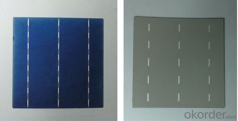
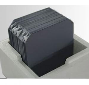
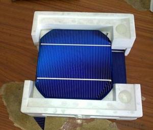
MONO5'(125*125mm)165
Monocrystalline silicon solar cell
Physical Characteristics
Dimension: 125mm×125mm±0.5mm
Diagonal: 165mm±0.5mm
Thickness(Si): 200±20 μm
Front(-) Back(+)
Blue anti-reflecting coating(silicon nitride); Aluminum back surface field;
1.6mmwide bus bars; 2.5mm wide soldering pads;
Distance between bus bars: 61mm . Distance between bus bars :61mm .
Electrical Characteristics
Efficiency(%) | 19.40 | 19.20 | 19.00 | 18.80 | 18.60 | 18.40 | 18.20 | 18.00 | 17.80 | 17.60 | 17.40 | 17.20 |
Pmpp(W) | 2.97 | 2.94 | 2.91 | 2.88 | 2.85 | 2.82 | 2.79 | 2.76 | 2.73 | 2.70 | 2.67 | 2.62 |
Umpp(V) | 0.537 | 0.535 | 0.533 | 0.531 | 0.527 | 0.524 | 0.521 | 0.518 | 0.516 | 0.515 | 0.513 | 0.509 |
Impp(A) | 5.531 | 5.495 | 5.460 | 5.424 | 5.408 | 5.382 | 5.355 | 5.328 | 5.291 | 5.243 | 5.195 | 4.147 |
Uoc(V) | 0.637 | 0.637 | 0.636 | 0.635 | 0.633 | 0.630 | 0.629 | 0.629 | 0.628 | 0.626 | 0.626 | 0.625 |
Isc(A) | 5.888 | 5.876 | 5.862 | 5.848 | 5.839 | 5.826 | 5.809 | 5.791 | 5.779 | 5.756 | 5.293 | 5.144 |
FAQ:
Q:How can i get some sample?
A:Yes , if you want order ,sample is not a problem.
Q:How about your solar panel efficency?
A: Our product efficency around 17.25%~18.25%.
Q:What’s the certificate you have got?
A: we have overall product certificate of ISO9001/ISO14001/CE/TUV/UL
- Q: Can solar silicon wafers be used in underwater applications?
- Yes, solar silicon wafers can be used in underwater applications. They are designed to be waterproof and can withstand the effects of being submerged in water. However, proper sealing and protection measures need to be in place to prevent any damage or corrosion to the wafers.
- Q: What is the purpose of a busbar in a solar silicon wafer?
- The purpose of a busbar in a solar silicon wafer is to conduct and distribute the electrical current generated by the wafer to the external circuitry. It acts as a pathway for the flow of electricity, allowing for efficient collection and utilization of the generated power.
- Q: How is a backsheet attached to a solar silicon wafer?
- A backsheet is typically attached to a solar silicon wafer using a strong adhesive or encapsulant material. The backsheet is carefully positioned and secured onto the surface of the wafer, providing protection and insulation for the solar cells against environmental factors such as moisture, heat, and UV radiation.
- Q: How are solar silicon wafers affected by temperature gradients?
- Solar silicon wafers are indeed affected by temperature gradients. When exposed to temperature variations, the thermal expansion and contraction of the silicon wafer can cause mechanical stress, leading to cracks or even breakage. Additionally, temperature gradients can also impact the efficiency of the solar cells, as higher temperatures tend to decrease their performance. Therefore, it is crucial to carefully manage and control temperature gradients to ensure the longevity and optimal functioning of solar silicon wafers.
- Q: What is the role of a passivation layer in a solar silicon wafer?
- The role of a passivation layer in a solar silicon wafer is to reduce surface recombination and improve the efficiency of the solar cell. It acts as a protective coating that prevents unwanted chemical reactions, minimizes surface defects, and enhances the electrical properties of the silicon wafer. This passivation layer helps to increase the overall performance and lifespan of the solar cell.
- Q: How do solar silicon wafers perform in polluted environments?
- Solar silicon wafers generally perform well in polluted environments, although excessive pollution can have a negative impact on their efficiency. Dust, smog, and other pollutants can accumulate on the surface of the wafers, reducing the amount of sunlight that reaches the solar cells and thus decreasing their power output. Regular cleaning and maintenance can help mitigate the effects of pollution and ensure optimal performance of solar panels in polluted areas.
- Q: What are the main defects in solar silicon wafers?
- The main defects in solar silicon wafers include crystallographic defects such as dislocations, grain boundaries, and stacking faults. These defects can reduce the efficiency of solar cells by limiting the flow of electrons, causing recombination of charge carriers, and affecting the overall electrical properties of the wafers.
- Q: What is the average weight of a solar silicon wafer?
- The average weight of a solar silicon wafer is typically around 2 to 4 grams.
- Q: What is the purpose of a spectral response in a solar silicon wafer?
- The purpose of a spectral response in a solar silicon wafer is to measure and understand how the wafer responds to different wavelengths of light. This information is crucial in determining the efficiency and performance of the solar cell, as it helps in identifying the parts of the solar spectrum that the cell can effectively convert into electricity.
- Q: What is the role of solar silicon wafers in the overall solar energy system?
- Solar silicon wafers play a crucial role in the overall solar energy system as they are the key component in photovoltaic (PV) cells, which convert sunlight into electricity. These wafers, made from high-purity silicon, are responsible for absorbing sunlight and generating a flow of electrons, thus producing direct current (DC) electricity. They are the foundation of solar panels and are essential for harnessing solar energy on a large scale.
Send your message to us
Silicon Wafer Solar Cell Panels - High Quality A Grade Mono Crystalline 5V 18.4% Solar Cells
- Loading Port:
- Shanghai
- Payment Terms:
- TT OR LC
- Min Order Qty:
- 1000 pc
- Supply Capability:
- 100000 pc/month
OKorder Service Pledge
OKorder Financial Service
Similar products
Hot products
Hot Searches
Related keywords
