
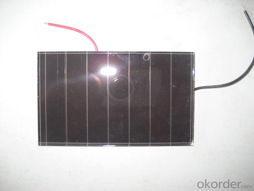
IC Grade Amorphous Silicon Dice Specification 3 Solar Silicon Wafer
- Ref Price:
-

- Loading Port:
- China Main Port
- Payment Terms:
- TT OR LC
- Min Order Qty:
- -
- Supply Capability:
- -
OKorder Service Pledge
OKorder Financial Service
You Might Also Like


Pv modules at present, the mainstream products are still in silicon as the main raw materials, only in terms of silicon raw material consumption, production 1 mw of crystalline silicon solar cell, need 10 to 12 tons of high purity silicon, but if use the same silicon materials used to produce thin film amorphous silicon solar cell can produce more than 200 mw.
From the perspective of energy consumption, amorphous silicon solar battery only 1-1.5 years of energy recovery period, more embodies its contribution to energy saving in the manufacturing process.
Component occupies a high proportion of costs in a photovoltaic system, the component prices directly affect the system cost, and thus affect the cost of photovoltaic power generation. Calculated at the current price of components, the same money, buy amorphous silicon products, you can get more close to 30% of the power components.
2, more power
For the same power of solar cell array, amorphous silicon solar cell is about 10% more than monocrystalline silicon, polycrystalline silicon battery power. This has been the Uni - Solar System LLC, Energy Photovoltaic Corp., Japan's Kaneka Corp., the Netherlands Energy research institute, and other organizations and experts confirmed that the Photovoltaic industry.
In sunny, that is to say, under the high temperature, amorphous silicon solar cell components can show more excellent power performance.
3, better low light response
Due to the characteristics of amorphous silicon atoms are arranged disorderly, the electron transition no longer comply with the restriction of traditional \"selection rule\", as a result, its light absorption characteristics and there are big differences monocrystalline silicon material. Amorphous silicon and monocrystalline silicon material absorption curve as shown
, amorphous silicon absorption curve has obvious three sections (A, B, C). Area A corresponding electronic transition between localized states, such as the gap state near Fermi level and to the tail state transition, the absorption coefficient is small, about 1-10 cm - 1, for this is absorbing; B area absorption coefficient with the increase of the photon energy index rose, it corresponds to the electrons from the valence band edge extension state to the conduction band localized state transition, as well as the localized electrons from the valence band tail states guide for edge extension state transition, the region's energy range is usually only about half of the electron volts, but absorption coefficient across two or three orders of magnitude, usually up to 104 cm - 1; Area C corresponds to the electrons from the valence band to the conduction band internal internal transition, the absorption coefficient is bigger, often in more than 104 cm - 1. After two absorption area is crystalline silicon eigen absorption area.
Can be seen in the figure, the intersection of two curves about 1.8 ev. It is important to note that in the visible light range (1.7 to 3.0 ev), the absorption coefficient of amorphous silicon material is almost an order of magnitude larger than the single crystal silicon. That is to say, in the morning the first part of the sun is not too strong, the second half, and it's cloudy in the afternoon under the condition of low light intensity, long wave is greater, the amorphous silicon material still has a large absorption coefficient. Again considering the amorphous silicon band gap is larger, the reverse saturation current I0 is smaller. And as mentioned the amorphous silicon battery the characteristics I - V characteristic curve of the amorphous silicon solar cell both in theory and in practical use in low light intensity has good adaptation.
• I - V characteristics of amorphous silicon cells after more than a Vm with the voltage drop slowly
In order to be convenient, we draw the I - V characteristics of two kinds of batteries on the same picture. Crystalline silicon and amorphous silicon battery I - V characteristics of general shape as shown
we see from the picture, two kinds of cells in the curve changes after exceed the maximum output power point gap is bigger. Output current of crystalline silicon cells after exceed the maximum output power point will soon fall to zero, curve steep; Rather than crystalline silicon cells output current after a long distance to fall to zero, the curve is relatively flat. Two kinds of battery Vm equivalent to about 83% of its open circuit voltage and 83% respectively.
when light intensity gradually become hour, short circuit current and open circuit voltage of solar battery will be stronger. Short circuit current decreases faster, of course, open circuit voltage decrease more slowly.
do in battery solar cell array under the condition of load, when the sun battery array of effective output voltage less than the terminal voltage of battery, battery cannot be recharged. When the light intensity gradually become hour, crystal silicon battery charging does not meet the conditions, and amorphous silicon due to the larger voltage difference, do not charge until the light is very dark, effectively increase the use of sunlight time. So, amorphous silicon cells to produce more electricity than the crystalline silicon.
4, more excellent high temperature performance
High in the outdoor environment temperature, amorphous silicon solar cell performance change, depends on the temperature, spectrum, as well as other related factors. But what is certain is: amorphous silicon than monocrystalline silicon or polycrystalline silicon are less likely to be affected by temperature.
Amorphous silicon solar cells than monocrystalline silicon, polycrystalline silicon cells have relatively small temperature coefficient of amorphous silicon solar cell output power best Pm temperature coefficient is about 0.19%, and monocrystalline silicon, polycrystalline silicon cells best output power Pm temperature coefficient is about 0.5%, when the battery work at higher temperatures, the two batteries will be a drop in the Pm, but the decline is different. They can be calculated using the following formula.
- Q: Monocrystalline silicon processing technology
- Wafer thickness is also a factor in productivity, as it relates to the number of wafers produced by each silicon block. The ultrathin wafer presents additional challenges to the wire technology, because the production process is much more difficult to. In addition to the mechanical brittleness of silicon wafers, if the wire sawing process no precise control, slight crack and bending will have negative effects on product yield. The system must be of ultra-thin silicon wire technology, linear cutting line speed and pressure, and precise control of cutting coolant.Regardless of the thickness of the silicon wafer, crystal silicon solar cell manufacturers have made great demands on the quality of the silicon wafer. The wafer cannot have surface damage (minor cracks, wire mark), morphology defects (bending, convex, uneven thickness) to minimize additional back-end processing such as polishing and other requirements to a minimum. Current situationIn order to meet the market for lower cost and higher productivity, a new generation of wire must improve the cutting speed, the use of silicon longer so as to improve the cutting load. Thinner cutting lines and thinner silicon chips increase productivity, while advanced process control can manage cutting line tension to keep the cutting line firm.
- Q: How are solar silicon wafers protected from external factors like moisture or dust?
- Solar silicon wafers are typically protected from external factors like moisture or dust by encapsulating them with a layer of protective materials. This encapsulation process involves laminating the wafers between two layers of transparent, durable materials such as glass or polymer sheets, which are then sealed together. This encapsulation not only provides a physical barrier against moisture and dust but also helps in maintaining the structural integrity and electrical performance of the solar cells. Additionally, the encapsulated wafers are often further protected by being placed within a weatherproof and resistant casing or frame to ensure long-term durability and protection from external elements.
- Q: How does a solar silicon wafer convert sunlight into electricity?
- A solar silicon wafer converts sunlight into electricity through a process called the photovoltaic effect. When sunlight hits the silicon wafer, it excites the electrons within the silicon atoms, causing them to break free and create an electric current. This current can then be harnessed and used as electricity.
- Q: 4 inch polished silicon wafer thickness of 250um, after polishing the thickness of 6 inches of 300um, the current use of wax free polishing process often fragments, to find a solution!
- I don't know how your employees operateYou can put a small bubble in the insertion box below if it is convenient. Can play a buffer role
- Q: How are solar silicon wafers tested for quality control?
- Solar silicon wafers are tested for quality control through a series of rigorous evaluations. These tests typically include visual inspections to detect any physical defects, such as cracks or impurities. Additionally, electrical measurements are conducted to assess the wafers' performance and efficiency. This may involve assessing parameters like resistivity, carrier lifetime, and dark current. Finally, wafers are subjected to optical measurements to analyze their reflectance, transmittance, and surface texturing. These comprehensive quality control tests ensure that only high-quality and reliable solar silicon wafers are used in the production of solar cells and modules.
- Q: What is the expected efficiency improvement for multi-junction solar silicon wafers?
- The expected efficiency improvement for multi-junction solar silicon wafers is typically around 30-40%.
- Q: Can solar silicon wafers be used in wearable fashion accessories?
- Yes, solar silicon wafers can be used in wearable fashion accessories. The small size and flexibility of these wafers make them suitable for integrating into accessories like smartwatches, bracelets, or even clothing items. By harnessing solar energy, these accessories can power various functionalities, such as charging small electronic devices or monitoring health metrics. Additionally, the use of solar silicon wafers aligns with the growing trend of sustainable fashion, making them an attractive option for eco-conscious consumers.
- Q: How do solar silicon wafers handle temperature variations?
- Solar silicon wafers are designed to handle temperature variations quite well. This is because they are typically made from high-quality materials that have been carefully engineered to withstand extreme temperatures. The wafers have a low coefficient of thermal expansion, meaning they expand and contract minimally with temperature changes. This helps to prevent cracking or damage to the wafers. Additionally, solar cells are often encapsulated in protective materials that provide insulation and help regulate temperature, further enhancing their ability to handle temperature variations.
- Q: What is the expected payback period for a solar panel with silicon wafers?
- The expected payback period for a solar panel with silicon wafers can vary depending on various factors such as the initial cost of the panel, its efficiency, the amount of sunlight it receives, and the local electricity rates. On average, solar panels with silicon wafers have a payback period ranging from 5 to 10 years, but this can be shorter in areas with high solar irradiation and favorable incentives or longer in areas with lower solar resource and limited incentives.
- Q: Can solar silicon wafers be used in agricultural irrigation systems?
- No, solar silicon wafers cannot be directly used in agricultural irrigation systems. However, solar panels made from silicon wafers can be used to generate electricity, which can then be used to power water pumps or other components of an agricultural irrigation system.
Send your message to us
IC Grade Amorphous Silicon Dice Specification 3 Solar Silicon Wafer
- Ref Price:
-
- Loading Port:
- China Main Port
- Payment Terms:
- TT OR LC
- Min Order Qty:
- -
- Supply Capability:
- -
OKorder Service Pledge
OKorder Financial Service
Similar products


Hot products


Hot Searches
Related keywords

