


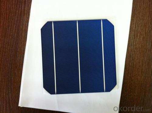


Silicon Wafer Solar Cell - High Quality A Grade Mono Crystalline 5V 17.2%
- Ref Price:
-

- Loading Port:
- Shanghai
- Payment Terms:
- TT OR LC
- Min Order Qty:
- 1000 pc
- Supply Capability:
- 100000 pc/month
OKorder Service Pledge
OKorder Financial Service
You Might Also Like


Specifications
hot sale solar cell
1.16.8%~18.25% high efficiency
2.100% checked quality
3.ISO9001/ISO14001/TUV/CE/UL
4.stable performance
We can offer you the best quality products and services, don't miss !
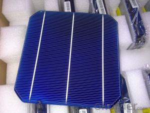
POLY6'(156*156)
Polycrystalline Silicon Solar cell
Physical Characteristics
Dimension: 156mm×156mm±0.5mm
Diagonal: 220mm±0.5mm
Thickness(Si): 200±20 μm
Front(-) Back(+)
Blue anti-reflecting coating (silicon nitride); Aluminum back surface field;
1.5mm wide bus bars; 2.0mm wide soldering pads;
Distance between bus bars: 51mm . Distance between bus bars :51mm .
Electrical Characteristics
Efficiency(%) | 18.00 | 17.80 | 17.60 | 17.40 | 17.20 | 16.80 | 16.60 | 16.40 | 16.20 | 16.00 | 15.80 | 15.60 |
Pmpp(W) | 4.33 | 4.29 | 4.24 | 4.19 | 4.14 | 4.09 | 4.04 | 3.99 | 3.94 | 3.90 | 3.86 | 3.82 |
Umpp(V) | 0.530 | 0.527 | 0.524 | 0.521 | 0.518 | 0.516 | 0.514 | 0.511 | 0.509 | 0.506 | 0.503 | 0.501 |
Impp(A) | 8.159 | 8.126 | 8.081 | 8.035 | 7.990 | 7.938 | 7.876 | 7.813 | 7.754 | 7.698 | 7.642 | 7.586 |
Uoc(V) | 0.633 | 0.631 | 0.628 | 0.625 | 0.623 | 0.620 | 0.618 | 0.617 | 0.615 | 0.613 | 0.611 | 0.609 |
Isc(A) | 8.709 | 8.677 | 8.629 | 8.578 | 8.531 | 8.478 | 8.419 | 8.356 | 8.289 | 8.220 | 8.151 | 8.083 |

MONO5'(125*125mm)165
Monocrystalline silicon solar cell
Physical Characteristics
Dimension: 125mm×125mm±0.5mm
Diagonal: 165mm±0.5mm
Thickness(Si): 200±20 μm
Front(-) Back(+)
Blue anti-reflecting coating(silicon nitride); Aluminum back surface field;
1.6mmwide bus bars; 2.5mm wide soldering pads;
Distance between bus bars: 61mm . Distance between bus bars :61mm .
Electrical Characteristics
Efficiency(%) | 19.40 | 19.20 | 19.00 | 18.80 | 18.60 | 18.40 | 18.20 | 18.00 | 17.80 | 17.60 | 17.40 | 17.20 |
Pmpp(W) | 2.97 | 2.94 | 2.91 | 2.88 | 2.85 | 2.82 | 2.79 | 2.76 | 2.73 | 2.70 | 2.67 | 2.62 |
Umpp(V) | 0.537 | 0.535 | 0.533 | 0.531 | 0.527 | 0.524 | 0.521 | 0.518 | 0.516 | 0.515 | 0.513 | 0.509 |
Impp(A) | 5.531 | 5.495 | 5.460 | 5.424 | 5.408 | 5.382 | 5.355 | 5.328 | 5.291 | 5.243 | 5.195 | 4.147 |
Uoc(V) | 0.637 | 0.637 | 0.636 | 0.635 | 0.633 | 0.630 | 0.629 | 0.629 | 0.628 | 0.626 | 0.626 | 0.625 |
Isc(A) | 5.888 | 5.876 | 5.862 | 5.848 | 5.839 | 5.826 | 5.809 | 5.791 | 5.779 | 5.756 | 5.293 | 5.144 |

FAQ:
Q:How can i get some sample?
A:Yes , if you want order ,sample is not a problem.
Q:How about your solar panel efficency?
A: Our product efficency around 17.25%~18.25%.
Q:What’s the certificate you have got?
A: we have overall product certificate of ISO9001/ISO14001/CE/TUV/UL
- Q: What is the role of surface recombination on solar silicon wafers?
- The role of surface recombination on solar silicon wafers is to reduce the efficiency of the solar cells. Surface recombination refers to the loss of charge carriers (electrons and holes) at the surface of the silicon wafer, which can significantly limit the performance of the solar cells. By reducing the surface recombination, the efficiency of the solar cells can be improved, leading to higher power output and better overall performance of the photovoltaic system.
- Q: How are solar silicon wafers handled and transported?
- Solar silicon wafers are typically handled and transported with great care to protect their fragile nature. They are usually packaged in protective cases or trays to prevent damage during handling and transportation. Specialized equipment, such as robotic arms or vacuum grippers, may be used to move and manipulate the wafers without causing any harm. Additionally, they are often transported in climate-controlled environments to prevent exposure to extreme temperatures or humidity, which can affect their performance.
- Q: How is a power output measured in a solar silicon wafer?
- A power output in a solar silicon wafer is typically measured by using a solar simulator to illuminate the wafer with a known intensity of light, and then measuring the electrical current and voltage produced by the wafer. The product of current and voltage gives the power output of the wafer.
- Q: Are solar silicon wafers affected by power fluctuations?
- Solar silicon wafers are not directly affected by power fluctuations. However, power fluctuations can impact the overall performance of the solar panels that incorporate these wafers. In such cases, voltage fluctuations can potentially affect the efficiency and output of the solar panels, but the silicon wafers themselves remain unaffected.
- Q: Why should the wafer cut side, cut out edge Jiaosha
- In fact, early silicon is not cutting edge, but with the development of microelectronics industry began the following reasons: cutting edge, W2) i: J n$W% L* M1 s `&;1, n can do a plurality of microelectronic devices on the wafer, cut down, and there is a crystal to crystal growth requirements, cutting along a direction for cutting chaos crack, cleavage is the professional said. The cutting edge tells you the direction of cleavage.2, N type and P type silicon wafer, a standard trimming is also inform you that it is n type or P type electrical characteristics, electrical characteristics, u$J2 z/ h 9 - O3, microelectronics production has been automated, such as lithography exposure if there is no cutting edge positioning, then the mask plate and the chip will be a difference of 180 degrees or a certain location, production efficiency will be very low...,4, the use of a lot of silicon, in addition to n/p also have crystal direction, for example, do MEMS requires corrosion anisotropy will be used <110> crystal direction, and MOS products in order to reduce the influence of the surface state requirements with <100> crystal...
- Q: How are solar silicon wafers handled and stored to prevent contamination?
- Solar silicon wafers are typically handled and stored in cleanroom environments to prevent contamination. These cleanrooms maintain controlled temperature, humidity, and air quality levels to minimize the presence of particles and pollutants. The wafers are usually stored in sealed containers or cassettes to protect them from dust, moisture, and other contaminants. Additionally, operators and technicians wear protective clothing, such as gloves and coveralls, to avoid direct contact and potential contamination of the wafers.
- Q: How do solar silicon wafers contribute to reducing air pollution?
- Solar silicon wafers contribute to reducing air pollution by enabling the production of clean and renewable energy. When sunlight hits the silicon wafers, it generates electricity without any harmful emissions or pollution. By replacing traditional fossil fuel-based energy sources with solar power, we can reduce the reliance on coal, oil, and gas, which are major contributors to air pollution.
- Q: Are solar silicon wafers affected by voltage fluctuations?
- Yes, solar silicon wafers can be affected by voltage fluctuations. Fluctuations in voltage can impact the performance and efficiency of solar cells, potentially leading to decreased power output. It is important to maintain stable and consistent voltage levels to optimize the performance of solar panels.
- Q: What is the impact of impurities on the performance of solar silicon wafers?
- The presence of impurities in solar silicon wafers can significantly impact their performance. Impurities can alter the electrical properties of the silicon, affecting the efficiency of the solar cell. For example, certain impurities can create energy barriers or recombination centers, reducing the overall conversion efficiency of the solar cell. Additionally, impurities can also lead to unwanted optical absorption, reducing the amount of light that can be absorbed and converted into electricity. Therefore, minimizing impurities and ensuring high-purity silicon wafers is crucial for maximizing the performance and efficiency of solar cells.
- Q: How is the demand for solar silicon wafers expected to grow in the future?
- The demand for solar silicon wafers is expected to grow significantly in the future due to the increasing adoption of solar energy as a sustainable and renewable source of power. As countries and industries shift towards clean energy solutions, the demand for solar panels, which heavily rely on silicon wafers, is projected to rise. Additionally, advancements in technology and manufacturing processes are likely to drive down costs, making solar power more accessible and further boosting the demand for silicon wafers.
Send your message to us
Silicon Wafer Solar Cell - High Quality A Grade Mono Crystalline 5V 17.2%
- Ref Price:
-
- Loading Port:
- Shanghai
- Payment Terms:
- TT OR LC
- Min Order Qty:
- 1000 pc
- Supply Capability:
- 100000 pc/month
OKorder Service Pledge
OKorder Financial Service
Similar products


Hot products


Hot Searches
Related keywords

