


Solar Mono Silicon Wafer for Solar Cell (156 and 125)
- Ref Price:
-

- Loading Port:
- China main port
- Payment Terms:
- TT or LC
- Min Order Qty:
- 10000 pc
- Supply Capability:
- 1000000 pc/month
OKorder Service Pledge
OKorder Financial Service
You Might Also Like


1. Structure of Solar Mono Silicon Wafer for Solar Cell (156 and 125) Description
A wafer, also called a slice or substrate, is a thin slice of semiconductor material, such as acrystalline silicon, used in electronics for the
fabrication of integrated circuits and in photovoltaics for conventional, wafer-based solar cells. The wafer serves as the substrate for
microelectronic devices built in and over the wafer and undergoes many microfabrication process steps such as doping or ion
implantation,etching, deposition of various materials, and photolithographic patterning. Finally the individual microcircuits are separated
(dicing) and packaged.
2. Main Features of the Solar Mono Silicon Wafer for Solar Cell (156 and 125)
• High quality Silicon wafer carrier box
• quartz glass wafer carrier from Taifulong Technology
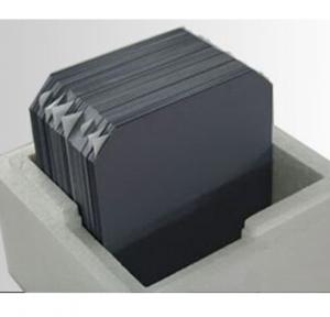
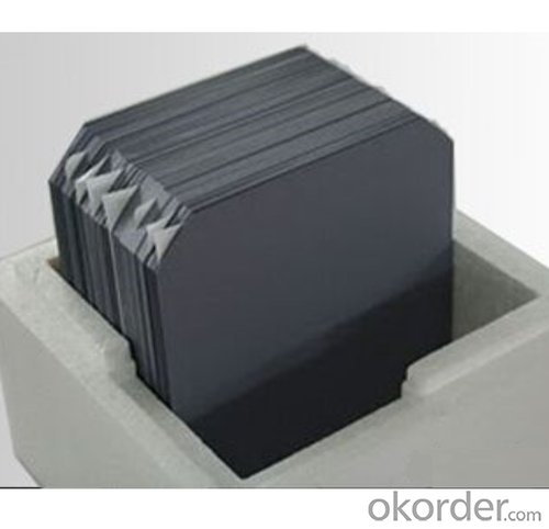
3. Solar Mono Silicon Wafer for Solar Cell (156 and 125) Images
")
")
4. Solar Mono Silicon Wafer for Solar Cell (156 and 125) Specification
窗体顶端 Item窗体底端 | N-type solar grade mono silicon wafer(125x125mm) | N-type solar grade mono silicon wafer(156x156mm) |
Growth Method | CZ | CZ |
Conductive Type | N-type | N-type |
Dopant | Phos. | Phos. |
Orientation | <100>±3° | <100>±3° |
Resistivity | 1 –3,3-6Ω•cm | 1 –3,3-6 Ω•cm |
Bulk Lifetime | ≥1000μs | ≥1000μs |
Oxygen Content | ≤0.1*1018 cm3 | ≤0.1*1018 cm3 |
Carbon Content | ≤0.1*1017 /cm3 | ≤0.1*1017 /cm3 |
Dimension | 125*125±0.5mm | 156*156±0.5mm |
Diagonal | 150±0.5mm | 200±0.5mm |
Square Sides Angle | 90±0.3° | 90±0.3° |
Thickness | 200±20 um | 200±20 um |
TTV | ≤25um | ≤25um |
Saw Mark | ≤15um | ≤15um |
Warp | ≤40um | ≤40um |
Chips | Depth<0.3mm;Length<0.5mm | Depth<0.3mm;Length<0.5mm, |
less than 2chips per wafer | less than 2chips per wafer | |
Appearance | No Stain, No Pinhole and Cracks by Visual Inspection | No Stain, No Pinhole and Cracks by Visual Inspection |
Dislocation Density | ≤1000 pcs/cm2 | ≤1000 pcs/cm2 |
Package | Packed in Polyethylene foam box,400pcs/box | Packed in Polyethylene foam box,400pcs/box 窗体底端 |
5. FAQ of Solar Mono Silicon Wafer for Solar Cell (156 and 125)
Q1. How long can we receive the product after purchase?
A1.In the purchase of product within three working days, We will arrange the factory delivery as soon as possible. The pecific time of receiving is related to the state and position of customers
Q2. Can we visit your factory?
A2:Surely, I will arrange the trip basing on your business schedule.
Q3:Which payment terms can you accept?
A3:T/T,L/C,Moneygram,Paypal are available for us.
- Q: Are solar silicon wafers affected by electromagnetic interference (EMI)?
- Yes, solar silicon wafers can be affected by electromagnetic interference (EMI). EMI can disrupt the electrical performance of solar cells, leading to reduced efficiency and output. Therefore, it is important to design solar installations with proper EMI mitigation measures in place to minimize any potential negative impacts.
- Q: What is the typical warranty period for a solar silicon wafer?
- The typical warranty period for a solar silicon wafer can vary, but it is commonly around 25 to 30 years.
- Q: How are solar silicon wafers protected from bird droppings?
- Solar silicon wafers are typically protected from bird droppings through the use of anti-reflective coatings or surface treatments. These coatings help to prevent bird droppings from sticking to the surface of the wafers, allowing them to be easily cleaned off without causing any damage. Additionally, regular maintenance and cleaning of solar panels can also help to minimize the impact of bird droppings and ensure optimal performance of the solar system.
- Q: What is the role of passivation on solar silicon wafers?
- The role of passivation on solar silicon wafers is to improve the efficiency and performance of the solar cells. Passivation involves the creation of a thin oxide layer on the surface of the silicon wafer, which acts as a protective barrier. This layer helps to reduce surface recombination, which is the loss of charge carriers, and prevents the formation of defects that can impair the cell's performance. Passivation also helps in maximizing the absorption of sunlight and enhances the overall electrical properties of the solar cell, resulting in higher conversion efficiency and improved long-term stability.
- Q: Mainly want to understand its physical principles and processing technology, thank you
- What we're talking about is charging or discharging a capacitor,The capacitance of the electricity is not easy to put the end, in theory, is to be able to 100 years, in fact, and there are different, which is why some of the memory card for a long time on the bad reasonProcessing technology is not easy to say, anyway, there is no level in China, the study did not useProbably and CPU processing technology is the same
- Q: How does the efficiency of a solar silicon wafer vary with different light conditions?
- The efficiency of a solar silicon wafer varies with different light conditions. In general, the efficiency tends to increase with higher light intensity and direct sunlight. However, factors such as the angle of incidence, temperature, and wavelength of the light can also influence the efficiency.
- Q: What is the production capacity of solar silicon wafers worldwide?
- As of 2021, the global production capacity of solar silicon wafers is estimated to be around 200 gigawatts (GW) per year.
- Q: What is the thickness of a solar silicon wafer?
- The thickness of a solar silicon wafer typically ranges from 150 to 200 micrometers.
- Q: How long does it take to produce a solar silicon wafer?
- The production of a solar silicon wafer typically takes around 2-3 weeks from start to finish.
- Q: Are solar silicon wafers affected by snow or ice accumulation?
- Yes, solar silicon wafers can be affected by snow or ice accumulation. When snow or ice covers the surface of the solar panels, it reduces the amount of sunlight reaching the silicon wafers, which decreases their efficiency. Additionally, the weight of heavy snow or ice can put strain on the panels and potentially cause damage if not cleared.
Send your message to us
Solar Mono Silicon Wafer for Solar Cell (156 and 125)
- Ref Price:
-
- Loading Port:
- China main port
- Payment Terms:
- TT or LC
- Min Order Qty:
- 10000 pc
- Supply Capability:
- 1000000 pc/month
OKorder Service Pledge
OKorder Financial Service
Similar products


Hot products


Hot Searches
Related keywords

