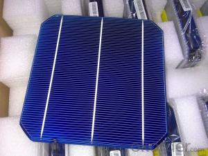


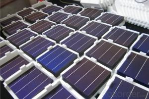
Silicon Wafer in Solar Cell - High Quality A Grade Mono Crystalline 5V 18.0% Solar Cell
- Ref Price:
-

- Loading Port:
- Shanghai
- Payment Terms:
- TT OR LC
- Min Order Qty:
- 1000 pc
- Supply Capability:
- 100000 pc/month
OKorder Service Pledge
OKorder Financial Service
You Might Also Like


Specifications
hot sale solar cell
1.16.8%~18.25% high efficiency
2.100% checked quality
3.ISO9001/ISO14001/TUV/CE/UL
4.stable performance
We can offer you the best quality products and services, don't miss !
POLY6'(156*156)
Polycrystalline Silicon Solar cell
Physical Characteristics
Dimension: 156mm×156mm±0.5mm
Diagonal: 220mm±0.5mm
Thickness(Si): 200±20 μm
Front(-) Back(+)
Blue anti-reflecting coating (silicon nitride); Aluminum back surface field;
1.5mm wide bus bars; 2.0mm wide soldering pads;
Distance between bus bars: 51mm . Distance between bus bars :51mm .
Electrical Characteristics
Efficiency(%) | 18.00 | 17.80 | 17.60 | 17.40 | 17.20 | 16.80 | 16.60 | 16.40 | 16.20 | 16.00 | 15.80 | 15.60 |
Pmpp(W) | 4.33 | 4.29 | 4.24 | 4.19 | 4.14 | 4.09 | 4.04 | 3.99 | 3.94 | 3.90 | 3.86 | 3.82 |
Umpp(V) | 0.530 | 0.527 | 0.524 | 0.521 | 0.518 | 0.516 | 0.514 | 0.511 | 0.509 | 0.506 | 0.503 | 0.501 |
Impp(A) | 8.159 | 8.126 | 8.081 | 8.035 | 7.990 | 7.938 | 7.876 | 7.813 | 7.754 | 7.698 | 7.642 | 7.586 |
Uoc(V) | 0.633 | 0.631 | 0.628 | 0.625 | 0.623 | 0.620 | 0.618 | 0.617 | 0.615 | 0.613 | 0.611 | 0.609 |
Isc(A) | 8.709 | 8.677 | 8.629 | 8.578 | 8.531 | 8.478 | 8.419 | 8.356 | 8.289 | 8.220 | 8.151 | 8.083 |

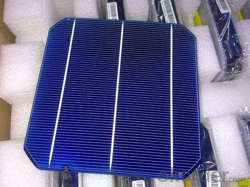
MONO5'(125*125mm)165
Monocrystalline silicon solar cell
Physical Characteristics
Dimension: 125mm×125mm±0.5mm
Diagonal: 165mm±0.5mm
Thickness(Si): 200±20 μm
Front(-) Back(+)
Blue anti-reflecting coating(silicon nitride); Aluminum back surface field;
1.6mmwide bus bars; 2.5mm wide soldering pads;
Distance between bus bars: 61mm . Distance between bus bars :61mm .
Electrical Characteristics
Efficiency(%) | 19.40 | 19.20 | 19.00 | 18.80 | 18.60 | 18.40 | 18.20 | 18.00 | 17.80 | 17.60 | 17.40 | 17.20 |
Pmpp(W) | 2.97 | 2.94 | 2.91 | 2.88 | 2.85 | 2.82 | 2.79 | 2.76 | 2.73 | 2.70 | 2.67 | 2.62 |
Umpp(V) | 0.537 | 0.535 | 0.533 | 0.531 | 0.527 | 0.524 | 0.521 | 0.518 | 0.516 | 0.515 | 0.513 | 0.509 |
Impp(A) | 5.531 | 5.495 | 5.460 | 5.424 | 5.408 | 5.382 | 5.355 | 5.328 | 5.291 | 5.243 | 5.195 | 4.147 |
Uoc(V) | 0.637 | 0.637 | 0.636 | 0.635 | 0.633 | 0.630 | 0.629 | 0.629 | 0.628 | 0.626 | 0.626 | 0.625 |
Isc(A) | 5.888 | 5.876 | 5.862 | 5.848 | 5.839 | 5.826 | 5.809 | 5.791 | 5.779 | 5.756 | 5.293 | 5.144 |

FAQ:
Q:How can i get some sample?
A:Yes , if you want order ,sample is not a problem.
Q:How about your solar panel efficency?
A: Our product efficency around 17.25%~18.25%.
Q:What’s the certificate you have got?
A: we have overall product certificate of ISO9001/ISO14001/CE/TUV/UL
- Q: What is the purpose of a grounding wire in a solar silicon wafer?
- The purpose of a grounding wire in a solar silicon wafer is to provide a path for excess electrical charge to safely dissipate into the ground. This helps to protect the wafer and other components of the solar system from damage caused by electrical surges or lightning strikes.
- Q: How does the efficiency of a solar silicon wafer change with altitude?
- The efficiency of a solar silicon wafer generally increases with altitude. This is because at higher altitudes, there is less atmospheric interference, such as air pollution and cloud cover, which can obstruct sunlight. As a result, solar panels at higher altitudes receive more direct and intense sunlight, leading to a higher energy output and increased efficiency of the silicon wafer.
- Q: Such as the title, look at some of the information, said the integrated circuit are integrated in silicon, why? Why not integrate on insulator?
- Another image, that is, the integrated circuit is a combination of some electronic components and wiring, no insulation and insulation as a support. It is achieved by adding bias and other techniques to isolate.And for why it's cheaper to use silicon, it's not because of its semiconductor nature that it uses it. The formation of P and N, a multi hole, a multi electron, and thus the role of different doping. GaAs expensive, but the performance is good, mostly for high-speed circuits and military aspects.
- Q: Can solar silicon wafers be used in portable solar panels?
- Yes, solar silicon wafers can be used in portable solar panels.
- Q: How does the efficiency of a solar silicon wafer change with snow cover?
- The efficiency of a solar silicon wafer generally decreases with snow cover. The snow layer acts as an insulator, preventing sunlight from reaching the wafer and reducing the amount of energy that can be converted into electricity. Additionally, the presence of snow can cause shading and reflection, further reducing the efficiency of the solar panel.
- Q: Can solar silicon wafers be used in solar-powered streetlights?
- Yes, solar silicon wafers can be used in solar-powered streetlights. These wafers are commonly used in the production of solar panels, which can generate electricity from sunlight. By integrating solar panels with streetlights, the solar silicon wafers help convert solar energy into electrical energy, enabling the streetlights to operate using renewable power sources.
- Q: What is the impact of wafer surface quality on solar silicon wafer performance?
- The impact of wafer surface quality on solar silicon wafer performance is significant. A high-quality wafer surface ensures better light absorption and reduces energy loss due to reflections. It also helps in improving the efficiency of solar cells by minimizing recombination and enhancing charge carrier collection. Additionally, a smooth and defect-free surface enables better adhesion and electrical contact during the manufacturing process, leading to more reliable and durable solar panels.
- Q: How does the efficiency of a solar silicon wafer change with cloud cover?
- The efficiency of a solar silicon wafer decreases with increasing cloud cover. Clouds block or scatter sunlight, reducing the amount of solar energy reaching the wafer. As a result, the wafer receives less sunlight to convert into electricity, leading to a decrease in its overall efficiency.
- Q: What is a solar silicon wafer?
- A solar silicon wafer is a thin slice or disc made from crystalline silicon, which is the primary material used in the manufacturing of solar cells. These wafers serve as the foundation for solar cell production, as they are doped and processed to create the necessary electrical properties for converting sunlight into electricity through the photovoltaic effect.
- Q: How is a solar silicon wafer connected to other components in a solar panel?
- A solar silicon wafer is typically connected to other components in a solar panel through a process called soldering. Soldering involves using a soldering iron to melt solder, a metal alloy, and then applying it to the connections between the wafer and other components. This creates a strong electrical and mechanical bond, allowing for efficient transfer of electricity within the solar panel.
Send your message to us
Silicon Wafer in Solar Cell - High Quality A Grade Mono Crystalline 5V 18.0% Solar Cell
- Ref Price:
-
- Loading Port:
- Shanghai
- Payment Terms:
- TT OR LC
- Min Order Qty:
- 1000 pc
- Supply Capability:
- 100000 pc/month
OKorder Service Pledge
OKorder Financial Service
Similar products


Hot products


Hot Searches
Related keywords

