
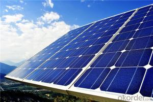
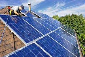
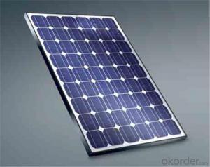


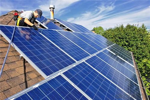

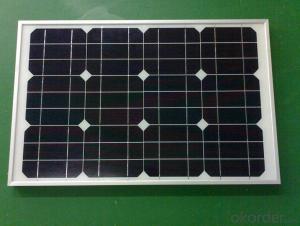
265W Industrial Silicon Wafer Solar Cells for Home Use Solar Power System
- Ref Price:
-

- Loading Port:
- China main port
- Payment Terms:
- TT OR LC
- Min Order Qty:
- 10000 watt
- Supply Capability:
- 20000000 watt/month
OKorder Service Pledge
OKorder Financial Service
You Might Also Like


Destription:
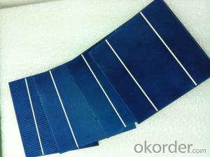
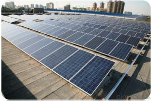
Solar panel refers to a panel designed to absorb the sun's rays as a source of energy for generating electricity or heating. A PV module is a packaged, connected assembly of typically 6×10 solar cells. Solar PV panels constitute the solar array of a photovoltaic system that generates and supplies solar electricity in commercial and residential applications.
Main Characteristic
1.Manufactured according to international quality and Environment Management
System (ISO9001, ISO14001)
2. By the high transmittance, low iron tempered glass, anti-aging of the EVA(polyethylene - vinyl acetate), high-performance crystalline silicon solar cells, good Weather resistance TPT (fluoroplastics composite membrane) by pyramid , has a good Weather resistance and anti-UV, hail, water-proof capacity.
3. OEM and customerized package are accepted
4. High efficiency crystalline silicon solar cells
Quality warranty
1.10 years limited warranty on material and workmanship
2. more than 90% power output in 10 years
3. more than 80% power output in 25 years
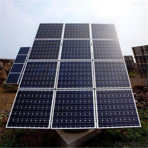
Product show


- Q: How is a mounting structure attached to a solar silicon wafer?
- A mounting structure is typically attached to a solar silicon wafer using a combination of adhesive materials and mechanical fasteners. The adhesive material, such as a specialized bonding agent or thermal conductive paste, helps to securely bond the mounting structure to the wafer's surface. Additionally, mechanical fasteners like screws or clips are used to provide additional stability and ensure a strong attachment between the mounting structure and the silicon wafer.
- Q: Are there any advancements in solar silicon wafer recycling technologies?
- Yes, there have been significant advancements in solar silicon wafer recycling technologies in recent years. Various methods such as mechanical, thermal, and chemical processes have been developed to efficiently recover and recycle silicon from discarded solar panels. These advancements aim to reduce waste, lower costs, and minimize the environmental impact of solar panel manufacturing and disposal.
- Q: Why should the wafer cut side, cut out edge Jiaosha
- In fact, early silicon is not cutting edge, but with the development of microelectronics industry began the following reasons: cutting edge, W2) i: J n$W% L* M1 s `&;1, n can do a plurality of microelectronic devices on the wafer, cut down, and there is a crystal to crystal growth requirements, cutting along a direction for cutting chaos crack, cleavage is the professional said. The cutting edge tells you the direction of cleavage.2, N type and P type silicon wafer, a standard trimming is also inform you that it is n type or P type electrical characteristics, electrical characteristics, u$J2 z/ h 9 - O3, microelectronics production has been automated, such as lithography exposure if there is no cutting edge positioning, then the mask plate and the chip will be a difference of 180 degrees or a certain location, production efficiency will be very low...,4, the use of a lot of silicon, in addition to n/p also have crystal direction, for example, do MEMS requires corrosion anisotropy will be used <110> crystal direction, and MOS products in order to reduce the influence of the surface state requirements with <100> crystal...
- Q: How is a solar silicon wafer tested for quality?
- A solar silicon wafer is tested for quality through various inspection methods. These include visual inspection to check for any visible defects such as cracks, scratches, or impurities on the surface. The electrical performance of the wafer is evaluated using techniques like resistivity measurement, which ensures the desired conductivity. Additionally, the wafer's thickness, flatness, and dimension are measured to ensure it meets the required specifications. These quality tests help determine the efficiency and reliability of the solar silicon wafer before it is used in solar cell production.
- Q: What are the applications of solar silicon wafers?
- Solar silicon wafers are primarily used in the production of solar cells, which are the building blocks of solar panels. These wafers serve as the foundation for the photovoltaic process, allowing sunlight to be converted into electricity. Additionally, solar silicon wafers can also be used in the manufacturing of other electronic devices, such as integrated circuits and semiconductors, due to their high purity and excellent electrical properties.
- Q: How do solar silicon wafers contribute to reducing greenhouse gas emissions?
- Solar silicon wafers contribute to reducing greenhouse gas emissions by enabling the production of solar panels, which generate clean and renewable electricity. As silicon wafers are the key component of photovoltaic cells, they absorb sunlight and convert it into usable energy, eliminating the need for fossil fuel-based power generation. By replacing traditional energy sources with solar power, greenhouse gas emissions from power plants and other fossil fuel combustion processes are significantly reduced, consequently mitigating climate change and promoting a more sustainable future.
- Q: How is a junction box integrated into a solar silicon wafer?
- A junction box is typically integrated into a solar silicon wafer by being attached to the backside of the wafer. The junction box houses the electrical connections and components necessary for the solar panel to function, such as diodes, bypass diodes, and connectors. It is securely sealed to protect the components from environmental factors and ensure reliable performance.
- Q: What is the purpose of a junction box in a solar silicon wafer?
- The purpose of a junction box in a solar silicon wafer is to provide a safe and secure enclosure for the electrical connections and components of the solar panel. It helps protect the wiring from environmental factors such as moisture and dust, and facilitates the connection of multiple solar panels in an array. Additionally, the junction box includes diodes that prevent reverse current flow, ensuring optimal performance and efficiency of the solar panel.
- Q: How long do solar silicon wafers last in a solar panel?
- Solar silicon wafers can last for several decades in a solar panel, typically around 25 to 30 years. However, their efficiency might gradually decline over time due to various factors such as exposure to sunlight, temperature fluctuations, and potential manufacturing defects. Regular maintenance and cleaning can help maximize the lifespan and performance of solar panels.
- Q: What is the impact of impurities on the performance of solar silicon wafers?
- Impurities can have a significant impact on the performance of solar silicon wafers. These impurities, such as metallic contaminants or dopants, can affect the electrical properties and overall efficiency of the wafers. They can introduce defects or alter the crystal structure, leading to reduced electron mobility, increased recombination rates, and lower conversion efficiencies. Therefore, minimizing impurities and maintaining high purity levels in solar silicon wafers is crucial for achieving optimal performance and maximizing the power output of solar cells.
Send your message to us
265W Industrial Silicon Wafer Solar Cells for Home Use Solar Power System
- Ref Price:
-
- Loading Port:
- China main port
- Payment Terms:
- TT OR LC
- Min Order Qty:
- 10000 watt
- Supply Capability:
- 20000000 watt/month
OKorder Service Pledge
OKorder Financial Service
Similar products

Hot products


Hot Searches
Related keywords

