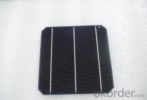


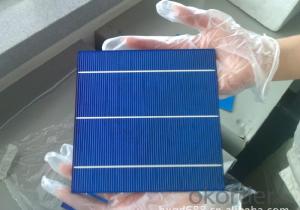
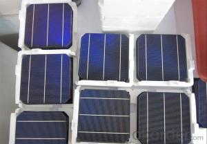
Silicone Wafer Solar Panel - High Quality A Grade Monocrystalline Solar Cell 5V 17.4%
- Ref Price:
-

- Loading Port:
- Shanghai
- Payment Terms:
- TT OR LC
- Min Order Qty:
- 1000 pc
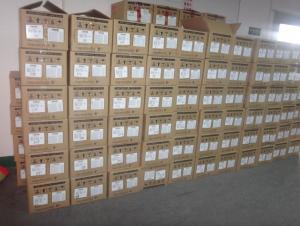
- Supply Capability:
- 100000 pc/month
OKorder Service Pledge
OKorder Financial Service
You Might Also Like


Specifications
hot sale solar cell
1.16.8%~18.25% high efficiency
2.100% checked quality
3.ISO9001/ISO14001/TUV/CE/UL
4.stable performance
We can offer you the best quality products and services, don't miss !
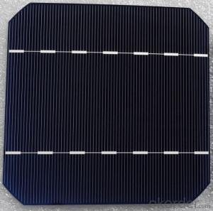
POLY6'(156*156)
Polycrystalline Silicon Solar cell
Physical Characteristics
Dimension: 156mm×156mm±0.5mm
Diagonal: 220mm±0.5mm
Thickness(Si): 200±20 μm
Front(-) Back(+)
Blue anti-reflecting coating (silicon nitride); Aluminum back surface field;
1.5mm wide bus bars; 2.0mm wide soldering pads;
Distance between bus bars: 51mm . Distance between bus bars :51mm .
Electrical Characteristics
Efficiency(%) | 18.00 | 17.80 | 17.60 | 17.40 | 17.20 | 16.80 | 16.60 | 16.40 | 16.20 | 16.00 | 15.80 | 15.60 |
Pmpp(W) | 4.33 | 4.29 | 4.24 | 4.19 | 4.14 | 4.09 | 4.04 | 3.99 | 3.94 | 3.90 | 3.86 | 3.82 |
Umpp(V) | 0.530 | 0.527 | 0.524 | 0.521 | 0.518 | 0.516 | 0.514 | 0.511 | 0.509 | 0.506 | 0.503 | 0.501 |
Impp(A) | 8.159 | 8.126 | 8.081 | 8.035 | 7.990 | 7.938 | 7.876 | 7.813 | 7.754 | 7.698 | 7.642 | 7.586 |
Uoc(V) | 0.633 | 0.631 | 0.628 | 0.625 | 0.623 | 0.620 | 0.618 | 0.617 | 0.615 | 0.613 | 0.611 | 0.609 |
Isc(A) | 8.709 | 8.677 | 8.629 | 8.578 | 8.531 | 8.478 | 8.419 | 8.356 | 8.289 | 8.220 | 8.151 | 8.083 |

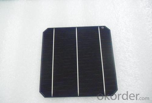
MONO5'(125*125mm)165
Monocrystalline silicon solar cell
Physical Characteristics
Dimension: 125mm×125mm±0.5mm
Diagonal: 165mm±0.5mm
Thickness(Si): 200±20 μm
Front(-) Back(+)
Blue anti-reflecting coating(silicon nitride); Aluminum back surface field;
1.6mmwide bus bars; 2.5mm wide soldering pads;
Distance between bus bars: 61mm . Distance between bus bars :61mm .
Electrical Characteristics
Efficiency(%) | 19.40 | 19.20 | 19.00 | 18.80 | 18.60 | 18.40 | 18.20 | 18.00 | 17.80 | 17.60 | 17.40 | 17.20 |
Pmpp(W) | 2.97 | 2.94 | 2.91 | 2.88 | 2.85 | 2.82 | 2.79 | 2.76 | 2.73 | 2.70 | 2.67 | 2.62 |
Umpp(V) | 0.537 | 0.535 | 0.533 | 0.531 | 0.527 | 0.524 | 0.521 | 0.518 | 0.516 | 0.515 | 0.513 | 0.509 |
Impp(A) | 5.531 | 5.495 | 5.460 | 5.424 | 5.408 | 5.382 | 5.355 | 5.328 | 5.291 | 5.243 | 5.195 | 4.147 |
Uoc(V) | 0.637 | 0.637 | 0.636 | 0.635 | 0.633 | 0.630 | 0.629 | 0.629 | 0.628 | 0.626 | 0.626 | 0.625 |
Isc(A) | 5.888 | 5.876 | 5.862 | 5.848 | 5.839 | 5.826 | 5.809 | 5.791 | 5.779 | 5.756 | 5.293 | 5.144 |

FAQ:
Q:How can i get some sample?
A:Yes , if you want order ,sample is not a problem.
Q:How about your solar panel efficency?
A: Our product efficency around 17.25%~18.25%.
Q:What’s the certificate you have got?
A: we have overall product certificate of ISO9001/ISO14001/CE/TUV/UL
- Q: What is the effect of temperature on the efficiency of a solar silicon wafer?
- The efficiency of a solar silicon wafer is directly influenced by temperature. As temperature increases, the efficiency of the wafer decreases. This is because the electrical characteristics of the silicon material change with temperature, leading to a decrease in the conversion of sunlight into electricity. Therefore, it is crucial to maintain optimal temperature conditions for a solar silicon wafer to maximize its efficiency and overall performance.
- Q: What is the role of solar silicon wafers in reducing water consumption?
- Solar silicon wafers play a crucial role in reducing water consumption by enabling the production of solar panels, which generate electricity without the need for water-intensive cooling systems. This helps alleviate the strain on water resources, as traditional power generation methods often require substantial amounts of water for cooling purposes.
- Q: What is the impact of wafer thickness on solar silicon wafer performance?
- The impact of wafer thickness on solar silicon wafer performance is significant. Thicker wafers tend to have lower resistivity, which allows for better electron flow and higher efficiency in converting sunlight into electricity. Additionally, thicker wafers provide better mechanical stability and can withstand higher temperatures and stress, improving the overall durability and reliability of solar cells. However, thicker wafers also increase material and manufacturing costs, making them less economically viable. Therefore, finding the optimal wafer thickness is crucial to balancing performance, cost, and efficiency in solar cell production.
- Q: What is the role of anti-reflective coating on solar silicon wafers?
- The role of anti-reflective coating on solar silicon wafers is to minimize the reflection of sunlight and increase the amount of light absorption by the silicon material. By reducing reflection, the coating allows more light to reach the silicon wafer, enhancing the efficiency of solar cells and ultimately improving the overall performance of the solar panel.
- Q: How are solar silicon wafers protected from transportation damage?
- Solar silicon wafers are protected from transportation damage through the use of specialized packaging materials and handling procedures. These wafers are typically placed in anti-static trays or boxes, which provide cushioning and prevent physical impact during transit. Additionally, shock-absorbing materials such as foam or bubble wrap may be used to further protect the wafers from vibrations or jolts. Furthermore, stringent quality control measures are implemented to ensure that the packaging is secure and that the wafers are not exposed to extreme temperatures or humidity, which could potentially damage their delicate structure.
- Q: How do solar silicon wafers perform in high-temperature environments?
- Solar silicon wafers are designed to perform well in high-temperature environments. They are made using materials that can withstand extreme heat without significant degradation. The wafers are engineered to have low thermal coefficients of expansion, which means they can expand and contract without cracking or losing their structural integrity. Additionally, solar cells are often encapsulated in protective materials that can handle high temperatures. Overall, solar silicon wafers have been proven to be reliable and efficient even in hot climates or during periods of intense sunlight.
- Q: Can solar silicon wafers be used in water pumping systems?
- Yes, solar silicon wafers can be used in water pumping systems. Solar silicon wafers are commonly used in photovoltaic panels to convert sunlight into electricity. By harnessing solar energy, these panels can power water pumping systems, allowing for sustainable and environmentally friendly water pumping solutions.
- Q: What factors contribute to the degradation of a solar silicon wafer?
- There are several factors that can contribute to the degradation of a solar silicon wafer. One of the main factors is exposure to environmental conditions such as humidity, temperature fluctuations, and UV radiation. These conditions can cause the silicon material to degrade over time, leading to a decrease in its efficiency and performance. Another factor is the presence of impurities or defects in the silicon wafer, which can affect its electrical properties and overall functionality. Additionally, improper handling during manufacturing, installation, or maintenance processes can also contribute to the degradation of the solar silicon wafer.
- Q: Can solar silicon wafers be used in solar-powered electric fences?
- Yes, solar silicon wafers can be used in solar-powered electric fences. The wafers are used in solar panels to convert sunlight into electricity, which can then power the electric fence system.
- Q: One hundred watts of solar panels to how many pieces of silicon wafers, 156 of single crystals and polycrystalline
- Whereas it is high. If we do not consider the area, the same power, the electricity generated is the same, with high conversion rate and low exchange rate independent of all aspects of life, of course, there will be some impact. So I do not know clearly? I is a professional manufacturer of solar photovoltaic, do not understand what I can find. If you can.
Send your message to us
Silicone Wafer Solar Panel - High Quality A Grade Monocrystalline Solar Cell 5V 17.4%
- Ref Price:
-
- Loading Port:
- Shanghai
- Payment Terms:
- TT OR LC
- Min Order Qty:
- 1000 pc
- Supply Capability:
- 100000 pc/month
OKorder Service Pledge
OKorder Financial Service
Similar products


Hot products


Hot Searches
Related keywords

