


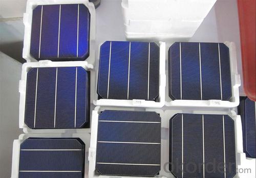

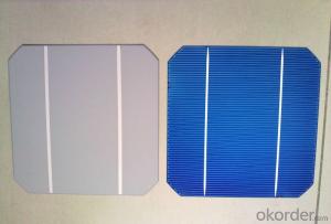
Silicon Wafer To Solar Cell - Mono Solar Cells 156mm*156mm in Bulk Quantity Low Price Stock 18.6
- Ref Price:
-

- Loading Port:
- Shanghai
- Payment Terms:
- TT OR LC
- Min Order Qty:
- 1000 pc
- Supply Capability:
- 100000 pc/month
OKorder Service Pledge
OKorder Financial Service
You Might Also Like


Brief Introduction
- Up to 20.0% efficiency, one of the highest performing mono crystalline cells on the market
- Three bus bars boosts current collection over the entire cell area, leading to higher fill factors
- Blue anti-reflecting coating allows more sunlight be captured and converted to electricity
- Finer, closer fingers improves charge collections for improved energy yield
- Lower light-induced degradation leads to greater power output over the entire module lifetime
- All solar cells are tightly classified to optimize output of module
- Maximum yield and longevity due to hotspot prevention
- Premium appearance results in a highly uniform and aesthetically appealing module
Specification
- Product Mono-crystalline silicon solar cell
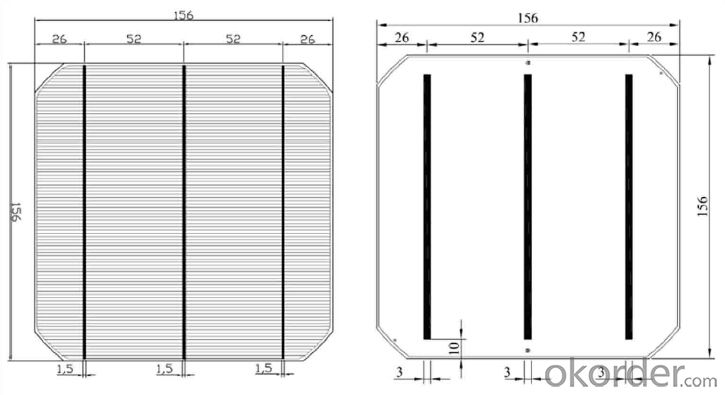
- Dimension 156 mm x 156 mm ± 0.5 mm
- Thickness 200 μm ± 30 μm
- Front 1.5 ± 0.1 mm busbar (silver)
- Silicon nitride antireflection coating
- Back 3.0 mm continuous soldering pads (silver)
- Back surface field (aluminum)
Electric performance parameters

- Testing conditions: 1000 W/m2, AM 1.5, 25 °C, Tolerance: Efficiency ± 0.2% abs., Pmpp ±1.5% rel.
- Imin : at 0.5 V
Light Intensity Dependence

Soldering Ability
- Peel Strength: > 1.0 N/mm (Pull soldered ribbon from busbar in 5 mm/s of 180°)
Dimension Figure

Quick Response
- Any time and anywhere, reply clients' email and solve all problems happen in the work at the first time.
- Remove clients doubts and offer the best solution at the first time.
- Give our clients the lastest news of the photovoltaic, update the newest stock informtion.
Production and Quality Control
- Precision cell efficiency sorting procedures
- Stringent criteria for color uniformity and appearance
- Reverse current and shunt resistance screening
- ISO9001,ISO14001 and OHSAS 18001,TUV Certificated


FAQ:
1. Q: Do you have your own factory?
A: Yes, we have. Our factory located in Jiangsu
2. Q: How can I visit your factory?
A: Before you visit,please contact us.We will show you the route or arrange a car to pick you up.
3. Q: Do you provide free sample?
A: Commenly we provide paid sample.
4. Q: Could you print our company LOGO on the nameplate and package?
A: Yes, we accept it.And need an Authorization Letter from you.
5. Q: Do you accept custom design on size?
A: Yes, if the size is reasonable.
6. Q: How can I be your agent in my country?
A: Please leave feedback. It's better for us to talk about details by email.
7. Q: Do you have solar project engineer who can guide me to install system?
A: Yes, we have a professional engineer team. They can teach you how to install a solar system.
- Q: How is the doping level of a solar silicon wafer controlled?
- The doping level of a solar silicon wafer is controlled through a process called ion implantation. In this process, specific dopant atoms are introduced into the silicon wafer by bombarding it with high-energy ions. The dopant atoms replace some of the silicon atoms in the crystal lattice, altering its electrical properties. The concentration and distribution of dopant atoms are carefully controlled to achieve the desired doping level, which helps in optimizing the performance of solar cells.
- Q: How does the efficiency of a solar silicon wafer change with altitude?
- The efficiency of a solar silicon wafer does not change significantly with altitude. Altitude primarily affects the intensity of sunlight, but it has a minimal impact on the efficiency of a solar silicon wafer. The main factors influencing efficiency are temperature, tilt, and shading, rather than altitude.
- Q: Are there any regulations or standards for solar silicon wafers?
- Yes, there are regulations and standards for solar silicon wafers. These regulations and standards are put in place to ensure the quality, efficiency, and safety of solar silicon wafers used in the production of solar cells and panels. They cover various aspects such as the purity of the silicon, thickness and uniformity of the wafer, electrical properties, and environmental sustainability. These regulations and standards are developed and enforced by organizations such as the International Electrotechnical Commission (IEC) and the American Society for Testing and Materials (ASTM). Compliance with these regulations and standards is important for the reliable and effective operation of solar energy systems.
- Q: Can solar silicon wafers be used in solar-powered charging stations?
- Yes, solar silicon wafers can be used in solar-powered charging stations. Solar silicon wafers are the primary component of solar panels, which generate electricity from sunlight. Solar-powered charging stations utilize solar panels to convert sunlight into electricity, which can be used to charge various devices. Therefore, solar silicon wafers are essential in enabling the functionality of solar-powered charging stations.
- Q: What is the expected lifetime of a solar silicon wafer?
- The expected lifetime of a solar silicon wafer varies depending on several factors such as its quality, manufacturing process, and usage conditions. Generally, high-quality silicon wafers used in solar panels are designed to have a long operational lifespan. They can typically last anywhere from 25 to 30 years or even more with proper maintenance.
- Q: Why should the wafer cut side, cut out edge Jiaosha
- To determine the crystal, cutting the adhesive carbon or glass, mounted on the fixed equipment.In simple terms is to determine the crystal direction, in order to facilitate future cutting, design graphics to consider this point, and then ask a little deeper, it is necessary to look at the book.Transistors in general with 111 sides, MOS general 110The reason for this is related to doping, corrosion and other post production, but also the activity of different layers of electrons is different, potential energy is not the same.
- Q: What is the price of monocrystalline silicon
- On a large grain of silicon, 160 thousand transistors can be integrated. What a fine project! This is the crystallization of multidisciplinary collaborative efforts, is another milestone in the progress of science and technology.
- Q: I would like to ask the unit in the production of silicon production line workers do harm to the body? (is the production of monocrystalline silicon, polycrystalline silicon photovoltaic enterprises)
- You are asking whether this problem is more harmful to the body is broad, if you ask whether they produce toxic substances will wafer production process, I can tell you: the wafer production involves no chemical reaction, no poison produced.
- Q: How are solar silicon wafers protected from extreme weather events?
- Solar silicon wafers are protected from extreme weather events through the use of specialized materials and coatings. These protective layers shield the wafers from moisture, temperature fluctuations, and other environmental factors that could potentially damage them. Additionally, solar panels are designed to withstand high winds and heavy rain, ensuring their resilience during storms and other severe weather conditions.
- Q: What is the average reflectivity of a solar silicon wafer?
- The average reflectivity of a solar silicon wafer is typically around 30%.
Send your message to us
Silicon Wafer To Solar Cell - Mono Solar Cells 156mm*156mm in Bulk Quantity Low Price Stock 18.6
- Ref Price:
-
- Loading Port:
- Shanghai
- Payment Terms:
- TT OR LC
- Min Order Qty:
- 1000 pc
- Supply Capability:
- 100000 pc/month
OKorder Service Pledge
OKorder Financial Service
Similar products


Hot products


Hot Searches
Related keywords

