


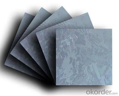

Silicon Solar Wafer
- Ref Price:
-

- Loading Port:
- China Main Port
- Payment Terms:
- TT OR LC
- Min Order Qty:
- -
- Supply Capability:
- -
OKorder Service Pledge
Quality Product, Order Online Tracking, Timely Delivery
OKorder Financial Service
Credit Rating, Credit Services, Credit Purchasing
You Might Also Like


Specifications
IC grade mono silicon wafer
1.Used in various discrete devices
2.High Purity 11N
3.Growth Method :CZ
![]()
| IC grade mono silicon wafer | ||
| Size | 4"/5"/6" | |
| Growth method | CZ | |
| Grade | Prime grade | |
| Diameter | 100±0.4mm / 125±0.5mm / 150±0.5mm | |
| Orientation | <111>/<100> | |
| Type | N-type/P-type | |
| Dopant | P-type:Boron | |
| N-type:Phos./As./Sb. | ||
| Purity | 11N(99.999999999%) | |
| Oxygen Content | ≤18 New PPMA | |
| Carborn Content | ≤1 New PPMA | |
| Resistivity | ≥0.001Ω·cm | |
| Thickness | ≥200um, or according to your requirement | |
| Others | TTV≤10um, Bow≤35um,Warp≤35um | |
| Particles | ≥0.3um@≤10PPW | |
| Surface | Frond side polished,back side etched. | |
| MOQ | 100pcs | |
| Package | Packed in cassette,and sealed in vacuum bag,25pcs/cassette. | |
| Price | According to your specification,especially resistivity and thickness | |


- Q: Are there any regulations or standards for solar silicon wafers?
- Yes, there are regulations and standards for solar silicon wafers. These standards are established by various organizations such as the International Electrotechnical Commission (IEC) and the American Society for Testing and Materials (ASTM). These standards ensure the quality, efficiency, and reliability of solar silicon wafers, covering factors such as dimensions, electrical properties, and material purity. Compliance with these regulations and standards is crucial for the solar industry to maintain consistency and facilitate widespread adoption of solar technology.
- Q: How do impurities affect the performance of a solar silicon wafer?
- Impurities in a solar silicon wafer can significantly impact its performance. These impurities, such as metal contaminants or non-uniform dopants, can create defects in the crystal lattice of the wafer, leading to reduced efficiency in converting sunlight into electricity. They can trap charge carriers, hinder electron movement, and cause recombination, resulting in decreased conductivity and lower power output. Therefore, minimizing impurities and ensuring high-purity silicon is crucial for optimizing the performance of a solar silicon wafer.
- Q: The higher the resistivity of silicon wafers, the better?!!! 1 experts please answer me!
- Low resistivity is helpful to improve the opening pressure, high resistivity and help to improve the short-circuit current, the best match between the two is about 1 -3! Own understanding!
- Q: How are solar silicon wafers protected from vandalism?
- Solar silicon wafers are typically protected from vandalism by installing them in secure locations, such as rooftops or fenced-off areas, that are difficult for unauthorized individuals to access. Additionally, some solar installations may employ security cameras, alarms, or other monitoring systems to deter and detect any potential acts of vandalism.
- Q: How is a spectral response measured in a solar silicon wafer?
- A spectral response in a solar silicon wafer is typically measured using a specialized instrument called a solar simulator. This instrument produces light with known characteristics, similar to sunlight, and illuminates the silicon wafer. The response of the wafer to different wavelengths of light is then measured using a photovoltaic (PV) characterization system, which can determine the efficiency and performance of the wafer across the solar spectrum.
- Q: What is the effect of surface texturing on solar silicon wafers?
- Surface texturing on solar silicon wafers has a positive effect on their efficiency and performance. It helps to increase light absorption by reducing the reflection of incident sunlight, leading to a higher conversion of solar energy into electricity. Additionally, surface texturing enhances the overall electrical conductivity of the wafers, improving their electrical performance. Thus, surface texturing plays a crucial role in enhancing the efficiency and output of solar cells.
- Q: Consult the difference between silicon and battery
- From the silicon wafer to the battery piece needs to undergo the process of making wool, and the single crystal silicon wafer is generally made of alkali. Therefore, the appearance of monocrystalline silicon battery is black, and the appearance of polycrystalline silicon sheet is dark blue.
- Q: Are solar silicon wafers affected by lightning strikes?
- Yes, solar silicon wafers can be affected by lightning strikes. Lightning strikes can cause physical damage to solar panels, including the silicon wafers, by melting or cracking them. Additionally, the high electrical currents associated with lightning strikes can potentially damage the electrical components of the solar panel system, such as the inverters. Therefore, it is important for solar panel installations to have proper lightning protection measures in place to minimize the risk of damage.
- Q: How does the efficiency of a solar silicon wafer change with panel orientation?
- The efficiency of a solar silicon wafer can change with panel orientation. The orientation and tilt angle of the solar panel can affect the amount of sunlight it receives, which directly impacts its efficiency. Ideally, a solar panel should be oriented to face the sun directly and tilted at an angle that maximizes sunlight absorption. If the panel is not properly oriented or tilted, it may receive less sunlight, leading to a decrease in efficiency.
- Q: Can solar silicon wafers be used in other electronic devices?
- Yes, solar silicon wafers can be used in other electronic devices. While they are primarily used in solar panels to convert sunlight into electricity, they can also be used in various other electronic applications such as sensors, integrated circuits, and batteries. The properties of solar silicon wafers, such as their high purity and efficient light absorption, make them suitable for a wide range of electronic devices beyond just solar panels.
Send your message to us
Silicon Solar Wafer
- Ref Price:
-
- Loading Port:
- China Main Port
- Payment Terms:
- TT OR LC
- Min Order Qty:
- -
- Supply Capability:
- -
OKorder Service Pledge
Quality Product, Order Online Tracking, Timely Delivery
OKorder Financial Service
Credit Rating, Credit Services, Credit Purchasing
Similar products


Hot products


Hot Searches

