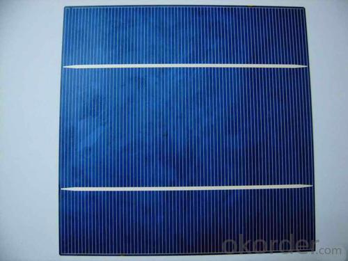
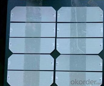
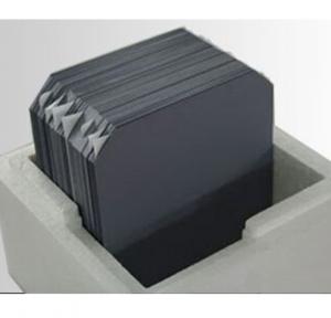
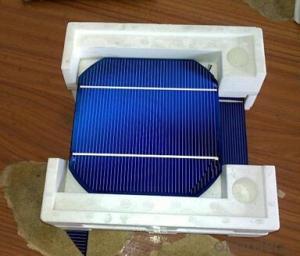
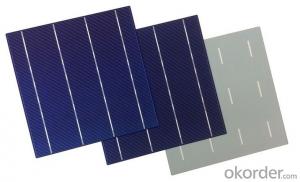
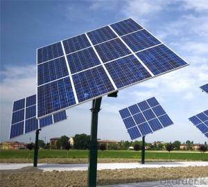
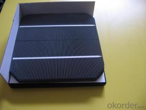
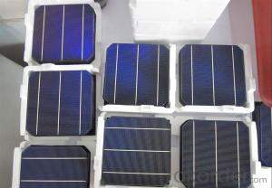
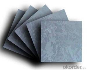
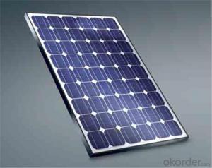
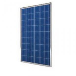
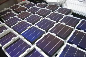
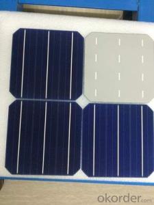
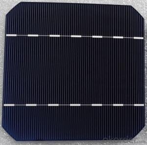
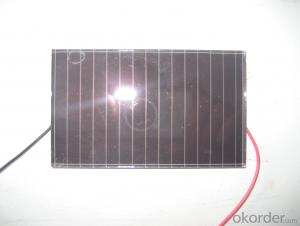
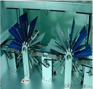
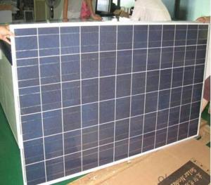
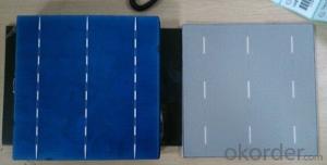
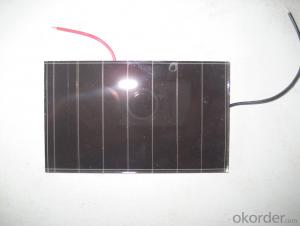
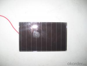
6*6 High Efficiency Mono Silicon Solar Panel Silicon Wafer
- Loading Port:
- China main port
- Payment Terms:
- TT OR LC
- Min Order Qty:
- 100 watt
- Supply Capability:
- 10000 watt/month
OKorder Service Pledge
OKorder Financial Service
You Might Also Like
Solar Module Summarize
Solar Module is the core part of solar PV power systems,also is the highest value part of it. The function of Solor Module is to convert the sun's radiation to electrical energy, or transfer it to battery and store in it, or to drive the load running.
The Product has been widely used in space and ground, it mainly used for power generation systems, charging systems, road lighting and traffic signs areas. It could offer a wide range of power and voltage, and with high conversion efficiency, and long service life.
Main Characteristic
17.6%-18% High Efficiency A Grade 125mm Monocrystalline Solar Cells
1.First-class production technology and packaging technology.
2.Adopting the world's leading technology of silicon and polycrystalline silicon cells, power density, peak hours more battery power, higher conversion efficiency.
3.Beautiful, stable, easy to take down the anodic aluminum frame electric degrees and has a wind-resistant, anti-snow function.
Features
17.6%-18% High Efficiency A Grade 125mm Monocrystalline Solar Cells
1.High transmissivity low-iron tempered glass, strong aluminium frame.
2.Manufactured according to international quality and Environment Management System (ISO9001, ISO14001).
3.Low voltage-temperature coefficient allows higher power output at high-temperature condition.
Product Pictures
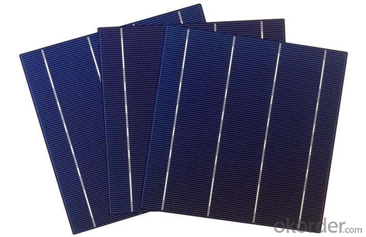
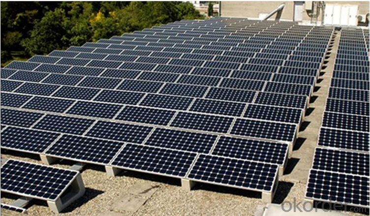
- Q: How are solar silicon wafers used in solar panels?
- Solar silicon wafers are the key component in solar panels as they serve as the substrate on which solar cells are built. These wafers are made from purified silicon and are typically sliced into thin, circular discs. Once the wafers are produced, they undergo several processes, such as doping and passivation, to enhance their electrical properties. The solar cells, which are composed of multiple layers including the silicon wafer, absorb sunlight and convert it into electricity through the photovoltaic effect. This electricity is then collected and utilized or stored for various applications.
- Q: Silicon on the thumb nail cap so large, the need for viscosity less than 20, the complete curing time of 1-2 days, you know, let's talk about it, grateful!
- The viscosity requirement is so small, why the curing time is so long, the general curing time is long anaerobic adhesive, or structural adhesive.
- Q: What is the role of passivation in solar silicon wafers?
- The role of passivation in solar silicon wafers is to minimize surface recombination and increase the efficiency of the solar cell. Passivation helps to create a protective layer on the surface of the wafer, reducing defects and allowing for better charge carrier flow, which ultimately improves the performance of the solar cell.
- Q: Can solar silicon wafers be used in solar-powered water pumps?
- Yes, solar silicon wafers can be used in solar-powered water pumps. These wafers are typically used in the production of solar panels, which capture sunlight and convert it into electricity. Solar-powered water pumps utilize this electricity to power the pump and move water without the need for an external power source.
- Q: How are solar silicon wafers protected from transportation damage?
- Solar silicon wafers are typically protected from transportation damage through various measures, such as packaging them in special containers or boxes that provide cushioning and shock absorption. These containers often include foam inserts or other materials that prevent the wafers from moving or vibrating during transit, minimizing the risk of breakage or cracking. Additionally, some manufacturers may use specialized handling procedures and equipment to ensure safe transportation of the wafers, reducing the potential for damage during loading, unloading, or movement.
- Q: What is the maximum power output of a solar silicon wafer?
- The maximum power output of a solar silicon wafer depends on various factors such as its size, efficiency, and environmental conditions. However, on average, a standard solar silicon wafer can produce around 4-5 watts of power per square inch.
- Q: How does the efficiency of a solar silicon wafer vary with different light conditions?
- The efficiency of a solar silicon wafer varies with different light conditions. Generally, the efficiency is highest when the wafer is exposed to direct, intense sunlight. However, the efficiency may decrease in low light conditions, such as during cloudy or overcast days, as there is less solar energy available to be converted into electricity. Additionally, extreme heat or shade can also negatively impact the efficiency of the silicon wafer. Overall, the efficiency of a solar silicon wafer is directly influenced by the intensity and quality of the light it receives.
- Q: Can solar silicon wafers be used in solar-powered streetlights?
- Yes, solar silicon wafers can be used in solar-powered streetlights. These wafers are commonly used in the production of solar panels, which capture sunlight and convert it into electricity. Solar-powered streetlights rely on solar panels to generate the necessary power to light up the streets. Therefore, solar silicon wafers play a crucial role in enabling the use of solar energy for street lighting.
- Q: What are the main challenges in the production of solar silicon wafers?
- One of the main challenges in the production of solar silicon wafers is the high energy consumption involved in the manufacturing process. The production of silicon wafers requires a significant amount of energy, particularly during the purification and crystallization stages. This poses a challenge in terms of the environmental impact and the overall sustainability of the process. Another challenge is the high cost associated with producing high-quality silicon wafers. The fabrication process requires precise control over various parameters such as temperature, pressure, and impurity levels, which can be expensive to maintain. Additionally, the raw materials used in the production, such as high-purity silicon, are costly, further adding to the overall production expenses. Furthermore, ensuring consistent and uniform quality across all produced wafers is another challenge. Variations in thickness, impurity levels, and crystal structure can have a significant impact on the efficiency and performance of solar cells. Thus, maintaining strict quality control measures throughout the production process is crucial but can be technically demanding and time-consuming. Lastly, the production of silicon wafers also generates a considerable amount of waste, including silicon dust and other byproducts. Proper disposal and recycling of these waste materials pose a challenge in terms of environmental sustainability and efficient resource management. Overall, addressing these challenges in energy consumption, cost, quality control, and waste management is essential to enhance the efficiency and sustainability of solar silicon wafer production.
- Q: How do solar silicon wafers perform in desert environments?
- Solar silicon wafers perform well in desert environments due to the high levels of sunlight and low humidity. The dry and hot conditions in deserts allow for efficient solar energy generation, as there are fewer obstructions such as clouds or pollution. However, it is important to ensure proper maintenance and cleaning of the wafers to prevent the accumulation of dust or sand particles, which can hinder their performance.
Send your message to us
6*6 High Efficiency Mono Silicon Solar Panel Silicon Wafer
- Loading Port:
- China main port
- Payment Terms:
- TT OR LC
- Min Order Qty:
- 100 watt
- Supply Capability:
- 10000 watt/month
OKorder Service Pledge
OKorder Financial Service
Similar products
Hot products
Hot Searches
Related keywords


