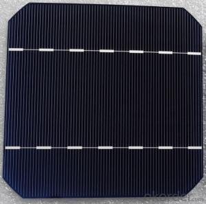


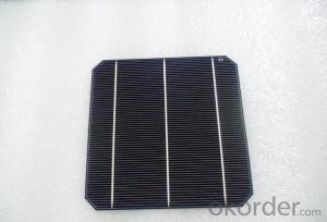
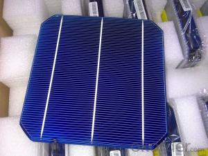
Silicon Wafer Solar Panel - High Quality A Grade Mono晶Silicon 5V 18.2% Solar Cell
- Ref Price:
-

- Loading Port:
- Shanghai
- Payment Terms:
- TT OR LC
- Min Order Qty:
- 1000 pc
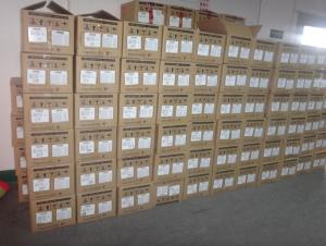
- Supply Capability:
- 100000 pc/month
OKorder Service Pledge
OKorder Financial Service
You Might Also Like


Specifications
hot sale solar cell
1.16.8%~18.25% high efficiency
2.100% checked quality
3.ISO9001/ISO14001/TUV/CE/UL
4.stable performance
We can offer you the best quality products and services, don't miss !
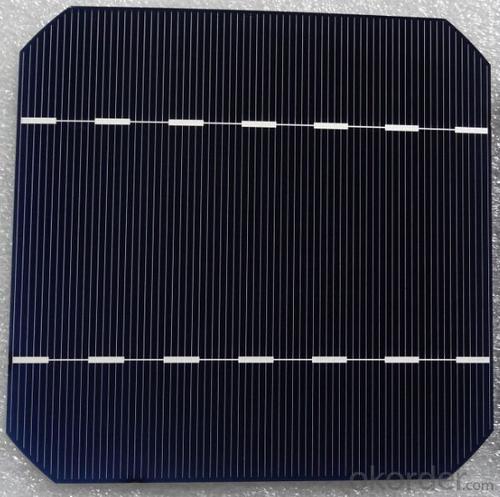
POLY6'(156*156)
Polycrystalline Silicon Solar cell
Physical Characteristics
Dimension: 156mm×156mm±0.5mm
Diagonal: 220mm±0.5mm
Thickness(Si): 200±20 μm
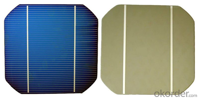
Front(-) Back(+)
Blue anti-reflecting coating (silicon nitride); Aluminum back surface field;
1.5mm wide bus bars; 2.0mm wide soldering pads;
Distance between bus bars: 51mm . Distance between bus bars :51mm .
Electrical Characteristics
Efficiency(%) | 18.00 | 17.80 | 17.60 | 17.40 | 17.20 | 16.80 | 16.60 | 16.40 | 16.20 | 16.00 | 15.80 | 15.60 |
Pmpp(W) | 4.33 | 4.29 | 4.24 | 4.19 | 4.14 | 4.09 | 4.04 | 3.99 | 3.94 | 3.90 | 3.86 | 3.82 |
Umpp(V) | 0.530 | 0.527 | 0.524 | 0.521 | 0.518 | 0.516 | 0.514 | 0.511 | 0.509 | 0.506 | 0.503 | 0.501 |
Impp(A) | 8.159 | 8.126 | 8.081 | 8.035 | 7.990 | 7.938 | 7.876 | 7.813 | 7.754 | 7.698 | 7.642 | 7.586 |
Uoc(V) | 0.633 | 0.631 | 0.628 | 0.625 | 0.623 | 0.620 | 0.618 | 0.617 | 0.615 | 0.613 | 0.611 | 0.609 |
Isc(A) | 8.709 | 8.677 | 8.629 | 8.578 | 8.531 | 8.478 | 8.419 | 8.356 | 8.289 | 8.220 | 8.151 | 8.083 |

MONO5'(125*125mm)165
Monocrystalline silicon solar cell
Physical Characteristics
Dimension: 125mm×125mm±0.5mm
Diagonal: 165mm±0.5mm
Thickness(Si): 200±20 μm
Front(-) Back(+)
Blue anti-reflecting coating(silicon nitride); Aluminum back surface field;
1.6mmwide bus bars; 2.5mm wide soldering pads;
Distance between bus bars: 61mm . Distance between bus bars :61mm .
Electrical Characteristics
Efficiency(%) | 19.40 | 19.20 | 19.00 | 18.80 | 18.60 | 18.40 | 18.20 | 18.00 | 17.80 | 17.60 | 17.40 | 17.20 |
Pmpp(W) | 2.97 | 2.94 | 2.91 | 2.88 | 2.85 | 2.82 | 2.79 | 2.76 | 2.73 | 2.70 | 2.67 | 2.62 |
Umpp(V) | 0.537 | 0.535 | 0.533 | 0.531 | 0.527 | 0.524 | 0.521 | 0.518 | 0.516 | 0.515 | 0.513 | 0.509 |
Impp(A) | 5.531 | 5.495 | 5.460 | 5.424 | 5.408 | 5.382 | 5.355 | 5.328 | 5.291 | 5.243 | 5.195 | 4.147 |
Uoc(V) | 0.637 | 0.637 | 0.636 | 0.635 | 0.633 | 0.630 | 0.629 | 0.629 | 0.628 | 0.626 | 0.626 | 0.625 |
Isc(A) | 5.888 | 5.876 | 5.862 | 5.848 | 5.839 | 5.826 | 5.809 | 5.791 | 5.779 | 5.756 | 5.293 | 5.144 |

FAQ:
Q:How can i get some sample?
A:Yes , if you want order ,sample is not a problem.
Q:How about your solar panel efficency?
A: Our product efficency around 17.25%~18.25%.
Q:What’s the certificate you have got?
A: we have overall product certificate of ISO9001/ISO14001/CE/TUV/UL
- Q: What is the expected future development of solar silicon wafers?
- The expected future development of solar silicon wafers is likely to focus on enhancing their efficiency, reducing production costs, and improving their durability. Technological advancements may include the development of high-efficiency wafers, such as tandem or multi-junction cells, which can capture a wider range of sunlight and convert it into electricity more effectively. Additionally, innovations in manufacturing processes, such as thinner wafers and new deposition techniques, may help reduce costs and increase production yields. Furthermore, efforts to enhance the durability of solar silicon wafers, making them more resistant to degradation and longer-lasting, will be crucial to ensure their long-term performance and economic viability.
- Q: Can solar silicon wafers be used in harsh climates?
- Yes, solar silicon wafers can be used in harsh climates. They are designed to withstand various environmental conditions, including extreme temperatures, humidity, and even exposure to dust and sand. Additionally, solar panels are tested and certified to ensure their durability and performance in harsh climates, making them suitable for use in such environments.
- Q: How are solar silicon wafers protected from environmental factors?
- Solar silicon wafers are protected from environmental factors through the use of encapsulation materials and coatings. These protective layers shield the wafers from moisture, dust, and other contaminants. Additionally, the wafers are often enclosed within a sturdy and sealed module, further safeguarding them from the elements.
- Q: What are the disadvantages of using solar silicon wafers?
- One major disadvantage of using solar silicon wafers is their high production cost. The process of manufacturing silicon wafers involves advanced technology and requires expensive materials, making the overall production expensive. Additionally, the extraction and purification of silicon from raw materials contribute to environmental concerns and energy consumption. Another drawback is their limited efficiency in converting sunlight into electricity, as silicon wafers have a lower absorption rate for certain wavelengths of light. This can lead to lower overall energy generation compared to other types of solar cells. Moreover, silicon wafers are rigid and bulky, making them less suitable for integration into flexible or lightweight devices.
- Q: What are the different materials used for passivation layers in solar silicon wafers?
- The different materials used for passivation layers in solar silicon wafers include silicon nitride (SiNx), aluminum oxide (Al2O3), and silicon oxide (SiO2). These materials are applied as thin films on the surface of the wafers to enhance their energy conversion efficiency and protect them from external factors such as moisture and contamination.
- Q: How do solar silicon wafers contribute to energy storage systems?
- Solar silicon wafers play a crucial role in energy storage systems by converting sunlight into electricity through the photovoltaic effect. These wafers, made from silicon crystals, absorb photons from sunlight and generate a flow of electrons, creating a direct current (DC) electrical output. This DC electricity can then be stored in batteries or converted into alternating current (AC) for immediate use or grid integration. Ultimately, solar silicon wafers facilitate the harnessing and storage of renewable energy, making them an essential component of energy storage systems.
- Q: Can solar silicon wafers be used in military applications?
- Yes, solar silicon wafers can be used in military applications. They can be utilized for powering remote military installations, charging batteries for electronic devices, and providing a renewable energy source for military operations in areas with limited access to conventional power grids.
- Q: Can solar silicon wafers be used in remote or inaccessible areas?
- Yes, solar silicon wafers can be used in remote or inaccessible areas. Solar panels made from silicon wafers are a popular choice for generating electricity in such areas as they can be easily transported and installed. Additionally, solar energy is a reliable and sustainable source of power, making it an ideal solution for remote locations where traditional power infrastructure may be absent or unreliable.
- Q: What is the average reflectivity of a solar silicon wafer?
- The average reflectivity of a solar silicon wafer is typically around 30%.
- Q: Can solar silicon wafers generate electricity in low light conditions?
- Yes, solar silicon wafers can generate electricity in low light conditions, although their efficiency may be reduced compared to direct sunlight.
Send your message to us
Silicon Wafer Solar Panel - High Quality A Grade Mono晶Silicon 5V 18.2% Solar Cell
- Ref Price:
-
- Loading Port:
- Shanghai
- Payment Terms:
- TT OR LC
- Min Order Qty:
- 1000 pc
- Supply Capability:
- 100000 pc/month
OKorder Service Pledge
OKorder Financial Service
Similar products


Hot products


Hot Searches
Related keywords

