


High Efficiency 6X6 Inch Silicon Wafer for Solar Cell
- Ref Price:
-

- Loading Port:
- Shanghai
- Payment Terms:
- TT OR LC
- Min Order Qty:
- 10000 pc
- Supply Capability:
- 200000 pc/month
OKorder Service Pledge
OKorder Financial Service
You Might Also Like


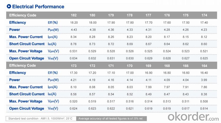
Quick Details | |||||
| Place of Origin: | China (Mainland) | Model Number: | 156P-2BB | ||
| Material:: | Polycrystalline Silicon | Size:: | 156mmx156mm or 6 inch | Max. Power:: | 4.2watts |
| efficiency:: | 16%-17.2% | busbar:: | 2 | Color: | Dark Blue |
| Voltage:: | 0.508V-0.53V | Thickness:: | 190um±20um | ||
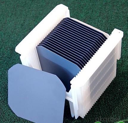
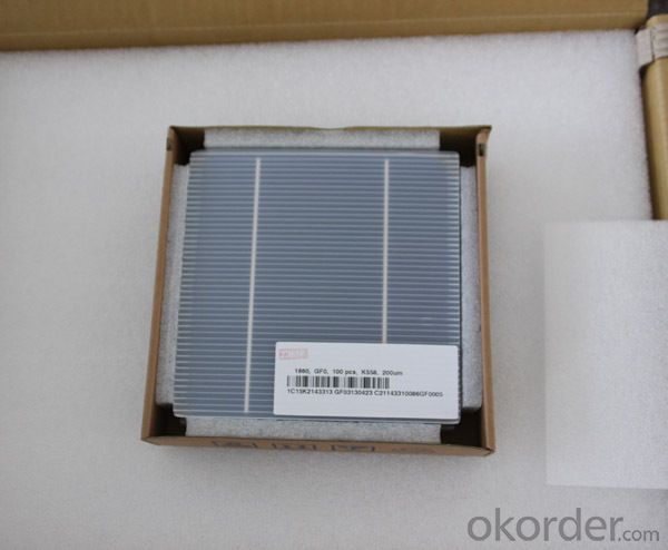
Packaging & Delivery
| Packaging Details: | 100pcs in one box,1000pcs per carton, standard export carton Silicon Wafer for Solar Cell |
| Delivery Detail: | 5-7 days after received the payment |
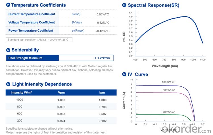
Specifications
Best Solar Cell Price
1.6*6 solar cell
2. 4.2W
3.2BB
Best Price Per Watt High Efficiency 6X6 Inch Silicon Wafer for Solar Cell
Product Description
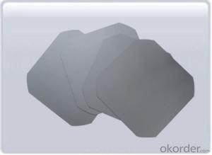
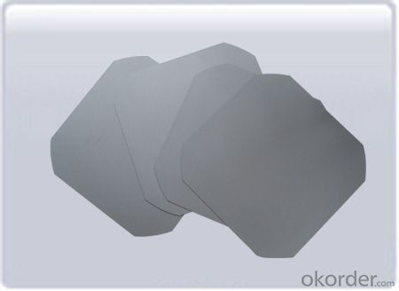
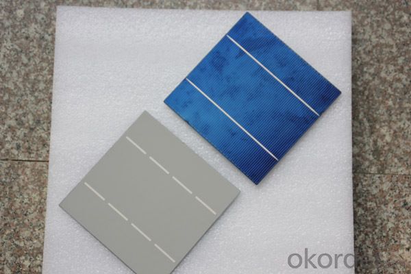
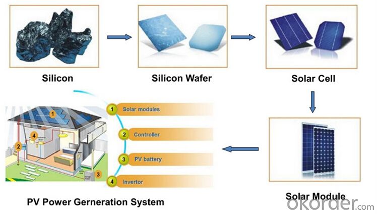
Silicon Wafer for Solar Cell
Dimension: 156x156mm
Front: Blue silicon nitride anti-reflection coating
2.0mm silver busbars
Back: Full-surface aluminum back-surface field
2.0mm( silver/ aluminum) discontinuous soldering pads
Image
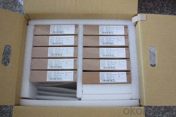
Packaging & Shipping
1. Item are only shipped after PAYMENT is received
2. Originally our solar cells are 100 pieces per box, 10 boxes per carton.
2. Please check out your ADDRESS carefully when processing order.
3. Please CONTACT us ASAP if you haven't received the parcel.
Shipping will be made via EMS, DHL, Fedex, UPS , TNT etc
- Q: In the silicon surface cleaning, there is a final step, the silicon chip into the 4% concentration of HF solution soak for five minutes, to hydrogen passivation treatment, and then rinse with deionized water after nitrogen drying,What is the role and mechanism of this hydrogen passivation?
- Wire cut damage layer thickness of 10 microns.Generally use 20% alkali solution in the corrosion condition at 90 C
- Q: Can solar silicon wafers be used in underwater applications?
- No, solar silicon wafers cannot be used in underwater applications as they are not designed to withstand the harsh conditions and pressure underwater.
- Q: How do solar silicon wafers contribute to the electrification of remote areas?
- Solar silicon wafers contribute to the electrification of remote areas by serving as a key component in solar panels. These panels harness the energy from the sun and convert it into electricity, providing a sustainable and reliable power source for off-grid communities. By using solar silicon wafers, remote areas can access clean and renewable energy, reducing their dependence on fossil fuels and improving their living conditions.
- Q: How are solar silicon wafers protected from chemical damage during manufacturing?
- Solar silicon wafers are protected from chemical damage during manufacturing through various methods. One common technique is the application of passivation layers, such as silicon nitride or silicon dioxide, which act as protective coatings. These layers prevent chemical reactions between the silicon and other substances, ensuring the wafers remain undamaged. Additionally, the manufacturing process may involve using cleanrooms with controlled environments to minimize the presence of potentially harmful chemicals. Quality control measures, including regular inspections and testing, are also implemented to ensure the wafers' protection from chemical damage throughout the manufacturing process.
- Q: What are the different types of junctions formed on solar silicon wafers?
- There are primarily three types of junctions formed on solar silicon wafers: p-n junctions, heterojunctions, and interdigitated back contact (IBC) junctions. P-n junctions are the most common, formed by doping one side of the wafer with a p-type material and the other side with an n-type material. Heterojunctions involve the use of different semiconductor materials to create the junction, typically combining silicon with a thin layer of another material like amorphous silicon or copper indium gallium selenide (CIGS). IBC junctions, on the other hand, have both the p-type and n-type regions on the same side of the wafer, allowing for improved efficiency and reduced shading.
- Q: How do solar silicon wafers contribute to energy security?
- Solar silicon wafers contribute to energy security by enabling the production of solar panels, which harness the abundant and renewable energy from the sun. This reduces dependence on fossil fuels and diversifies the energy mix, making it less vulnerable to price fluctuations and supply disruptions. Additionally, solar silicon wafers facilitate the decentralization of energy production, allowing households and businesses to generate their own electricity and rely less on centralized power grids. Overall, the use of solar silicon wafers promotes sustainable and reliable energy sources, enhancing energy security for individuals, communities, and countries.
- Q: How are solar silicon wafers protected from extreme weather events?
- Solar silicon wafers are protected from extreme weather events through various measures. One common method is the use of tempered glass, which acts as a protective barrier against hail, heavy rain, and snow. Additionally, the wafers are encapsulated with a layer of specialized materials, such as ethylene vinyl acetate (EVA), that provide insulation and resistance to temperature fluctuations. Moreover, the solar panels are designed to withstand high winds and are securely mounted to prevent damage from strong storms. All these precautions ensure that solar silicon wafers can endure and continue generating renewable energy even in harsh weather conditions.
- Q: What is the role of back surface field (BSF) in solar silicon wafers?
- The role of back surface field (BSF) in solar silicon wafers is to minimize the recombination of charge carriers, such as electrons and holes, at the back surface of the wafer. This is achieved by creating a high-doped layer at the back surface, which acts as a barrier for the charge carriers. By reducing recombination, BSF helps improve the overall efficiency of the solar cell by enhancing the collection of generated electrical current.
- Q: How is the voltage output of a solar silicon wafer regulated?
- The voltage output of a solar silicon wafer is regulated through the use of various components in a solar panel system. These components include a charge controller or regulator, which monitors and regulates the voltage and current flowing from the solar cells. It ensures that the voltage output remains within a safe and optimal range for the connected devices or battery being charged. Additionally, voltage regulators or inverters may be employed to further regulate and convert the DC voltage output of the solar cells into AC voltage suitable for use in household or grid-connected applications. Overall, these regulatory components play a crucial role in maintaining the stability and efficiency of the voltage output from a solar silicon wafer.
- Q: How to extract silicon from silicon wafers
- Slice: cut a single crystal silicon rod into a thin wafer with an exact geometry. In this process, the silica fume is produced by water leaching to produce waste water and silicon slag.
Send your message to us
High Efficiency 6X6 Inch Silicon Wafer for Solar Cell
- Ref Price:
-
- Loading Port:
- Shanghai
- Payment Terms:
- TT OR LC
- Min Order Qty:
- 10000 pc
- Supply Capability:
- 200000 pc/month
OKorder Service Pledge
OKorder Financial Service
Similar products


Hot products


Hot Searches
Related keywords

