


Monocrystalline Silicon Wafer,125*125, Solar Wafers
- Ref Price:
-

- Loading Port:
- Shanghai Port
- Payment Terms:
- TT or LC
- Min Order Qty:
- 100 Pieces PCS
- Supply Capability:
- 700MW/Per Year PCS/month
OKorder Service Pledge
OKorder Financial Service
You Might Also Like


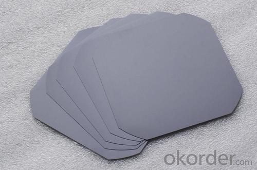
Specifications of Mono Solar Wafer
Monocrystalline solar wafer 125*125mm
Conductivity Type: P type
Dopant: Boron
Resistivity: 1~3 ohm
thickness: 200um.
| Product name | Mono Wafer |
| Conductive type | P type |
| Square size wafer(mm) | 125×125±0.5 mm |
| Resistivity | 1~3 ohm |
| Corner(mm) | 150±0.5;165±0.5 |
| 195±0.5;200±0.5 | |
| Thickness (μm) | 200±20 |
| Total thickness(um) | ≤ 30 |
| Resistivity range(Ωcm) | 1-3 |
| Doping elements | Boron |
| Orientation | (100)±1° |
| Carbon content(atoms/cc) | ≤1.0E+17 |
| Oxygen content(atoms/cc) | ≤1.0E+18 |
| Lifetime(μs) | ≥10 |
| Surface quality | No crack, gap, missing Angle, perforated, silicon fell and stress |
| Warping degrees(warp/μm) | ≤50 |
| Neighbouring vertical degree | 90±0.5° |
| Side damage(mm) | ≤0.5mm(length)×0.3mm(width)(not more than 2 per wafer) |
| Line mark(μm) | ≤15 |
Advantages of Mono Solar Wafers
1. High efficiency and High power.2. Long-term electrical stability.
3. Lowest price and Fastest delivery.
4. Good quality and good service.
5. Bulk supply
6. Good Warranty
7. Big Sale
8. More than 25 years on the lifetime.
Usage and Applications of Mono Solar Wafers
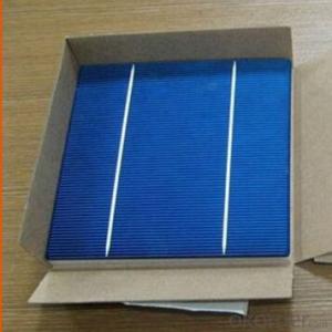
Mono Solar wafers is used to make Solar Cells. With high quality and stable quality. Our Solar Wafers can greatly improve the performance of Solar Cells.
Packaging & Delivery of Mono Solar Wafers
Carton Box Package and Deliver by air.It should be noticed that it should be avoid of water, sunshine and moist.
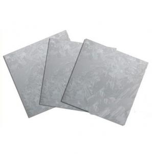
Wafer Factory Picture of Mono Solar Wafers

Package Picture of Mono Solar Wafers

- Q: What are the challenges in manufacturing large-sized silicon wafers?
- One of the primary challenges in manufacturing large-sized silicon wafers is maintaining uniformity and ensuring high-quality throughout the entire wafer. As the size of the wafer increases, it becomes more difficult to control factors like crystal growth, impurities, and defects, which can impact the overall performance of the integrated circuits. Additionally, handling and processing large-sized wafers require specialized equipment and techniques, increasing the cost and complexity of the manufacturing process.
- Q: Is a wafer a silicon wafer and a wafer?Please try to speak more popular, can be said to be made of silicon wafers do
- Ion implantation, etc., can be made into various semiconductor devices
- Q: What is the global production capacity of solar silicon wafers?
- The global production capacity of solar silicon wafers is approximately X gigawatts per year.
- Q: What is the meaning of a cleaning in a semiconductor silicon wafer process? RCA?
- () APM (SC-1): NH4OH/H2O2 /H2O 30 ~ 80 DEG C due to the action of H2O2, the surface of the silicon wafer has a natural oxide film (SiO2), which is hydrophilic, and the surface of the silicon wafer can be soaked with the cleaning liquid. Because the natural oxide layer on the surface of silicon wafer and the Si on the surface of silicon wafer are corroded by NH 4OH, the particles attached to the surface of the silicon wafer will fall into the cleaning liquid, so as to achieve the purpose of removing particles. At the same time, the H2O 2 forms a new oxide film on the surface of the oxidized silicon wafer when the NH4OH is etched on the surface of the silicon wafer.
- Q: Can solar silicon wafers be used in other electronic applications besides solar panels?
- Yes, solar silicon wafers can be used in other electronic applications besides solar panels. They are commonly used in various devices such as sensors, microprocessors, integrated circuits, and photovoltaic cells in electronic devices like calculators, smartphones, and laptops. The high purity and efficiency of solar silicon wafers make them suitable for a wide range of electronic applications beyond solar panels.
- Q: How much does a solar silicon wafer weigh?
- A solar silicon wafer typically weighs around 4-6 grams.
- Q: How are solar silicon wafers protected from electrical surges?
- Solar silicon wafers are protected from electrical surges through the use of protective devices such as surge arresters or varistors. These devices are connected in parallel with the solar cells and act as voltage clamps, diverting excess electrical energy away from the wafers. This helps prevent damage to the delicate silicon material and ensures the longevity and reliability of the solar panels.
- Q: What is the reason for the original or the original silicon?
- After the wafer is not cleaned clean, you should be monocrystalline wafers
- Q: Can solar silicon wafers be used in portable electronic devices?
- Yes, solar silicon wafers can be used in portable electronic devices. They can be integrated into the design of portable devices such as smartphones, tablets, and wearables to harness solar energy and provide a sustainable source of power. This enables the devices to charge their batteries using sunlight, increasing their energy efficiency and reducing the need for external power sources.
- Q: How efficient are solar silicon wafers in converting sunlight into electricity?
- Solar silicon wafers are highly efficient in converting sunlight into electricity. With advancements in technology, these wafers can now achieve conversion efficiencies of up to 25%. This means that they can convert 25% of the sunlight they receive into usable electrical energy, making them a reliable and effective choice for solar energy generation.
1. Manufacturer Overview
| Location | |
| Year Established | |
| Annual Output Value | |
| Main Markets | |
| Company Certifications |
2. Manufacturer Certificates
| a) Certification Name | |
| Range | |
| Reference | |
| Validity Period |
3. Manufacturer Capability
| a) Trade Capacity | |
| Nearest Port | |
| Export Percentage | |
| No.of Employees in Trade Department | |
| Language Spoken: | |
| b) Factory Information | |
| Factory Size: | |
| No. of Production Lines | |
| Contract Manufacturing | |
| Product Price Range | |
Send your message to us
Monocrystalline Silicon Wafer,125*125, Solar Wafers
- Ref Price:
-
- Loading Port:
- Shanghai Port
- Payment Terms:
- TT or LC
- Min Order Qty:
- 100 Pieces PCS
- Supply Capability:
- 700MW/Per Year PCS/month
OKorder Service Pledge
OKorder Financial Service
Similar products


Hot products


Hot Searches
Related keywords

