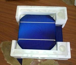
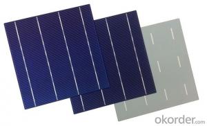
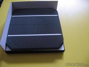
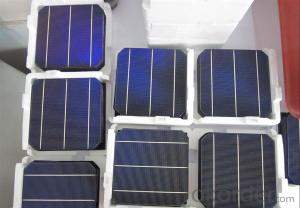
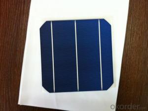
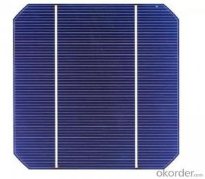
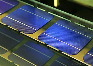
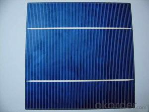
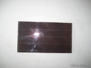
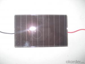
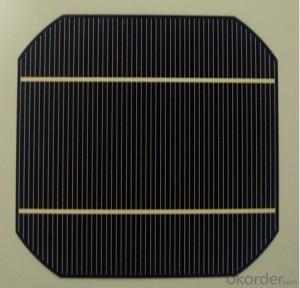
Solar Mono Silicon Wafer 5Watt-300Watt Mono Solar Cell
- Loading Port:
- China main port
- Payment Terms:
- TT OR LC
- Min Order Qty:
- 100 watt
- Supply Capability:
- 10000 watt/month
OKorder Service Pledge
OKorder Financial Service
You Might Also Like
Solar panel 5W-300W mono solar cell
Solar Module Summarize
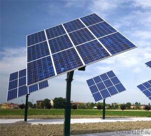
Solar Module is the core part of solar PV power systems,also is the highest value part of it. The function of Solor Module is to convert the sun's radiation to electrical energy, or transfer it to battery and store in it, or to drive the load running.
The Product has been widely used in space and ground, it mainly used for power generation systems, charging systems, road lighting and traffic signs areas. It could offer a wide range of power and voltage, and with high conversion efficiency, and long service life.
Main Characteristic
Long Service Life
High Efficiency Solar Cells
Special Aluminum Frame Design
High Transmission, Low Iron Tempered Glass
Advanced Cell Encapsulation
APPLICATIONS
Solar power stations
Rural electrification, Small home power systems
Power supply for traffic, security, gas industry
12V and 24V battery charging system
Other industrial and commercial application
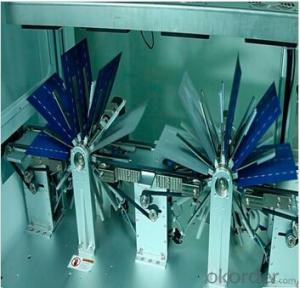
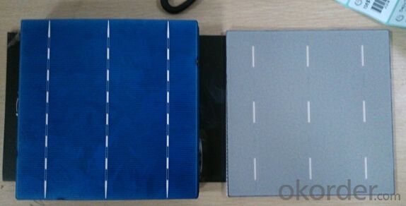
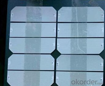
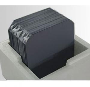
Product Show
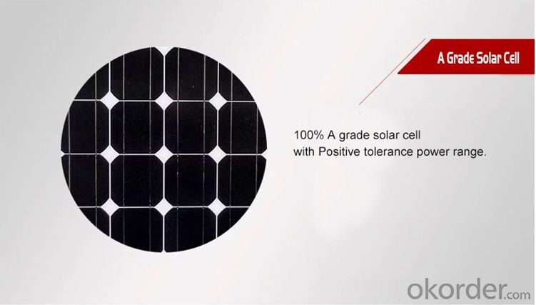
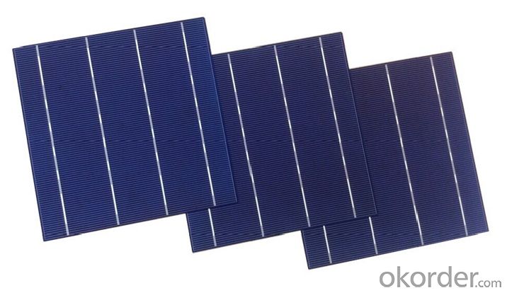

Warranties
6Inch 2BB Polycrystalline Multi Solar Cells Mono Solar Cell
For c-Si panel: 25years output warranty for no less than 80% of performance, 10 years output warranty for no less than 90% of performance. Free from material and workmanship defects within 5 years.
For a-Si panel: 20 years output warranty for no less than 80% of performance, 10 years output warranty for no less than 90% of performance. Free from material and workmanship defects within 2 years.
- Q: Can solar silicon wafers be used in off-grid applications?
- Yes, solar silicon wafers can be used in off-grid applications. Off-grid applications refer to systems or devices that are not connected to the main electrical grid and rely on alternative sources of power. Solar silicon wafers, when used in conjunction with other components such as solar cells, can capture sunlight and convert it into electricity, making them an ideal choice for generating power in off-grid scenarios.
- Q: Can solar silicon wafers be used in solar water heating systems?
- Yes, solar silicon wafers can be used in solar water heating systems. These wafers are commonly used in photovoltaic (PV) solar panels to convert sunlight into electricity. However, they can also be utilized in solar thermal systems, including solar water heating, where the sunlight is directly used to heat water.
- Q: Can solar silicon wafers be used in electric vehicle charging infrastructure?
- Yes, solar silicon wafers can be used in electric vehicle charging infrastructure. They can be used to generate solar power that is then converted into electrical energy to charge electric vehicles. This can provide a sustainable and renewable energy source for charging stations, reducing the dependence on traditional energy sources and minimizing the environmental impact of electric vehicle charging.
- Q: What is the meaning of the wafer (100), the crystal orientation index or the crystal plane index?Also (1100 and (111) which direction and angle should be cut?
- Said the origin and the point of x = 1, y = 1, the linear Z on the =1 atoms, if the crystal is body centered cubic lattice, the crystal orientation through the cube on the diagonal of the atom.
- Q: Are solar silicon wafers flexible?
- No, solar silicon wafers are not flexible. They are typically rigid and brittle in nature.
- Q: Who is the best silicon chip dryer?
- In general, the oil bath furnace heating a little more stable, St. steel technology to give me a more profound sense of the sale, the response time is relatively fast, and the service attitude is better, we can be anxious customers anxious.
- Q: Can solar silicon wafers be used in solar-powered wearable devices?
- Yes, solar silicon wafers can be used in solar-powered wearable devices. The wafers can be integrated into the design of wearable devices such as smartwatches, fitness trackers, or even clothing, to harness sunlight and convert it into electrical energy to power the device.
- Q: Why can silicon chips store information? Even if it is a miniature circuit, unplug the power on the use of electricity, there is no electricity in the silicon chip, in the form of what capacity storage
- So when you need to save the power. As you say the iron, can be used to save the information - the tape is the use of micro magnets to record
- Q: Can solar silicon wafers be used in solar-powered cell towers?
- Yes, solar silicon wafers can be used in solar-powered cell towers. These wafers are commonly used in the production of solar panels, which convert sunlight into electricity. Solar-powered cell towers utilize similar technology to harness solar energy and power their operations. By utilizing solar silicon wafers, cell towers can generate clean and renewable energy, reducing their reliance on traditional power sources.
- Q: How does the crystal structure of a solar silicon wafer affect its performance?
- The crystal structure of a solar silicon wafer plays a crucial role in determining its performance. The arrangement of silicon atoms in the crystal lattice affects the material's electrical properties, such as its ability to absorb and convert sunlight into electricity. A highly ordered crystal structure with minimal defects allows for efficient electron movement, resulting in improved solar cell efficiency. Conversely, a disordered structure or a high concentration of defects can hinder electron flow, reducing the overall performance of the solar wafer.
Send your message to us
Solar Mono Silicon Wafer 5Watt-300Watt Mono Solar Cell
- Loading Port:
- China main port
- Payment Terms:
- TT OR LC
- Min Order Qty:
- 100 watt
- Supply Capability:
- 10000 watt/month
OKorder Service Pledge
OKorder Financial Service
Similar products
Hot products
Hot Searches
Related keywords
