


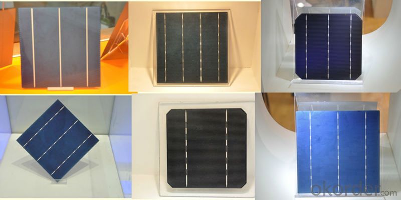


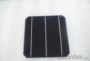
High Quality A Grade Monocrystalline Solar Grade Silicon Wafer Polycrystalline 5v 17.2% Solar Cell
- Ref Price:
-

- Loading Port:
- Shanghai
- Payment Terms:
- TT OR LC
- Min Order Qty:
- 1000 pc
- Supply Capability:
- 100000 pc/month
OKorder Service Pledge
OKorder Financial Service
You Might Also Like


Specifications
hot sale solar cell
1.16.8%~18.25% high efficiency
2.100% checked quality
3.ISO9001/ISO14001/TUV/CE/UL
4.stable performance
We can offer you the best quality products and services, don't miss !
POLY6'(156*156)
Polycrystalline Silicon Solar cell
Physical Characteristics
Dimension: 156mm×156mm±0.5mm
Diagonal: 220mm±0.5mm
Thickness(Si): 200±20 μm
Front(-) Back(+)
Blue anti-reflecting coating (silicon nitride); Aluminum back surface field;
1.5mm wide bus bars; 2.0mm wide soldering pads;
Distance between bus bars: 51mm . Distance between bus bars :51mm .
Electrical Characteristics
Efficiency(%) | 18.00 | 17.80 | 17.60 | 17.40 | 17.20 | 16.80 | 16.60 | 16.40 | 16.20 | 16.00 | 15.80 | 15.60 |
Pmpp(W) | 4.33 | 4.29 | 4.24 | 4.19 | 4.14 | 4.09 | 4.04 | 3.99 | 3.94 | 3.90 | 3.86 | 3.82 |
Umpp(V) | 0.530 | 0.527 | 0.524 | 0.521 | 0.518 | 0.516 | 0.514 | 0.511 | 0.509 | 0.506 | 0.503 | 0.501 |
Impp(A) | 8.159 | 8.126 | 8.081 | 8.035 | 7.990 | 7.938 | 7.876 | 7.813 | 7.754 | 7.698 | 7.642 | 7.586 |
Uoc(V) | 0.633 | 0.631 | 0.628 | 0.625 | 0.623 | 0.620 | 0.618 | 0.617 | 0.615 | 0.613 | 0.611 | 0.609 |
Isc(A) | 8.709 | 8.677 | 8.629 | 8.578 | 8.531 | 8.478 | 8.419 | 8.356 | 8.289 | 8.220 | 8.151 | 8.083 |

MONO5'(125*125mm)165
Monocrystalline silicon solar cell
Physical Characteristics
Dimension: 125mm×125mm±0.5mm
Diagonal: 165mm±0.5mm
Thickness(Si): 200±20 μm
Front(-) Back(+)
Blue anti-reflecting coating(silicon nitride); Aluminum back surface field;
1.6mmwide bus bars; 2.5mm wide soldering pads;
Distance between bus bars: 61mm . Distance between bus bars :61mm .
Electrical Characteristics
Efficiency(%) | 19.40 | 19.20 | 19.00 | 18.80 | 18.60 | 18.40 | 18.20 | 18.00 | 17.80 | 17.60 | 17.40 | 17.20 |
Pmpp(W) | 2.97 | 2.94 | 2.91 | 2.88 | 2.85 | 2.82 | 2.79 | 2.76 | 2.73 | 2.70 | 2.67 | 2.62 |
Umpp(V) | 0.537 | 0.535 | 0.533 | 0.531 | 0.527 | 0.524 | 0.521 | 0.518 | 0.516 | 0.515 | 0.513 | 0.509 |
Impp(A) | 5.531 | 5.495 | 5.460 | 5.424 | 5.408 | 5.382 | 5.355 | 5.328 | 5.291 | 5.243 | 5.195 | 4.147 |
Uoc(V) | 0.637 | 0.637 | 0.636 | 0.635 | 0.633 | 0.630 | 0.629 | 0.629 | 0.628 | 0.626 | 0.626 | 0.625 |
Isc(A) | 5.888 | 5.876 | 5.862 | 5.848 | 5.839 | 5.826 | 5.809 | 5.791 | 5.779 | 5.756 | 5.293 | 5.144 |

FAQ:
Q:How can i get some sample?
A:Yes , if you want order ,sample is not a problem.
Q:How about your solar panel efficency?
A: Our product efficency around 17.25%~18.25%.
Q:What’s the certificate you have got?
A: we have overall product certificate of ISO9001/ISO14001/CE/TUV/UL
- Q: How are solar silicon wafers interconnected to form solar modules?
- Solar silicon wafers are interconnected to form solar modules through a process called solar cell stringing. In this process, multiple silicon wafers are connected in series using metal conductive ribbons. The ribbons are soldered onto the front and back contacts of the adjacent wafers, creating an electrical pathway between them. This interconnection enables the flow of current generated by the individual solar cells, allowing them to work together efficiently and produce electricity.
- Q: How do solar silicon wafers contribute to reducing the reliance on imported energy?
- Solar silicon wafers contribute to reducing the reliance on imported energy by enabling the production of solar panels, which generate electricity from sunlight. By harnessing renewable energy sources like solar power, countries can reduce their dependence on imported fossil fuels and traditional energy sources. This shift towards locally produced solar energy helps to decrease the need for importing energy, leading to greater energy independence and reducing the strain on foreign energy supplies.
- Q: I would like to ask: silicon annealing treatment is how? Why anneal? Does annealing have an effect on the resistivity and the minority lifetime?
- Silicon wafer annealing process, is a part of the process. According to a certain procedure, the process of heating and cooling..;
- Q: The process for steel wire cutting silicon factory, we use HCTB5 wire, you can do?
- Product advantages of electroplated diamond wireCurrent line cutting methodInternal cuttingThe material utilization rate is only 40%~50%, and there are many defects, such as the wide kerf, the lower material, the poor precision of the surface shape, the depth of the surface damage layer and the size of the workpiece being machined.
- Q: What can be used to adjust its viscosity
- Polyethylene glycol and water soluble, I believe this may help you solve the problem
- Q: What is the role of junction boxes on solar silicon wafers?
- Junction boxes on solar silicon wafers serve as protective enclosures that house the electrical connections and components of a solar panel. They are responsible for managing the flow of electricity generated by the solar cells, ensuring proper connections, and providing protection against environmental factors such as moisture and dust. Additionally, junction boxes often include features like diodes and bypass capacitors to optimize the performance and safety of the solar panel.
- Q: Can solar silicon wafers be used in agricultural applications?
- Yes, solar silicon wafers can be used in agricultural applications. They can be utilized in solar-powered irrigation systems, water pumps, and other agricultural machinery to provide renewable energy and reduce reliance on fossil fuels. Additionally, solar panels made from silicon wafers can be installed on rooftops or open fields to generate electricity for agricultural operations, such as powering farm equipment and lighting.
- Q: Why can silicon chips store information? Even if it is a miniature circuit, unplug the power on the use of electricity, there is no electricity in the silicon chip, in the form of what capacity storage
- Storage of information is not a silicon chip, called memory, which is a transistor electronic components, called the silicon chip is made of silicon crystals directly on the transistor array,
- Q: What is the role of oxide layers on solar silicon wafers?
- The role of oxide layers on solar silicon wafers is to passivate the surface of the wafer and reduce recombination of charge carriers, thereby improving the efficiency of the solar cell.
- Q: How do solar silicon wafers perform in urban environments?
- Solar silicon wafers perform well in urban environments due to their ability to efficiently convert sunlight into electricity. However, certain factors such as shading from tall buildings and pollution can impact their performance. Overall, with proper installation and maintenance, solar silicon wafers can effectively generate renewable energy even in urban settings.
Send your message to us
High Quality A Grade Monocrystalline Solar Grade Silicon Wafer Polycrystalline 5v 17.2% Solar Cell
- Ref Price:
-
- Loading Port:
- Shanghai
- Payment Terms:
- TT OR LC
- Min Order Qty:
- 1000 pc
- Supply Capability:
- 100000 pc/month
OKorder Service Pledge
OKorder Financial Service
Similar products


Hot products


Hot Searches
Related keywords

