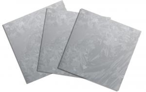

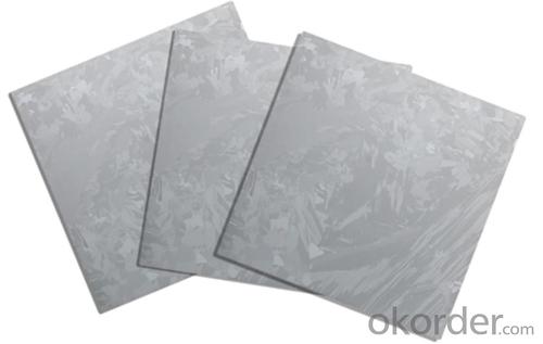

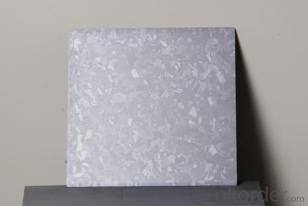
Silicon Wafer in Solar Photovoltaic Cells - Polycrystalline/Multiple Solar Silicon Wafer 156*156
- Ref Price:
-

- Loading Port:
- Shanghai Port
- Payment Terms:
- TT or LC
- Min Order Qty:
- 100 Pieces PCS
- Supply Capability:
- 700MW/Per Year PCS/month
OKorder Service Pledge
Quality Product, Order Online Tracking, Timely Delivery
OKorder Financial Service
Credit Rating, Credit Services, Credit Purchasing
You Might Also Like


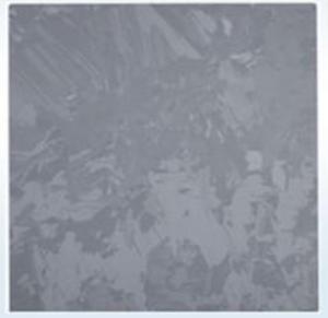
Specifications of Polycrystalline Silicon Wafer
Format : 156 mm × 156 mm ± 0.5 mm
Thickness : 200μm ± 10 μm
| Product name | Poly Wafer |
| Conductive type | P Type |
| Square size wafer (mm) | 156×156±0.5 |
| 219.20±0.5 | |
| Corner (mm)
|
1±0.5、45°±10º |
| 200±20 | |
| Total thickness(um) | ≤40 |
| Resistivity ranges(Ωcm) | 1-3 |
| Doping elements | boron |
| Carbon content(atoms/cc) | ≤8*1017 |
| Oxygen content(atoms/cc) | ≤1*1018 |
| Lifetime(μs) | ≥2 |
| Surface quality | No crack, gap, missing Angle, perforated, window, microcrystalline |
| Warping degrees(μm) | ≤50 |
| Neighbouring vertical degree | 90±0.5° |
| Side damage(mm) | ≤0.5mm(length)×0.3mm(width),(not more than 2 per wafer) |
| Line mark(μm) | ≤15 |
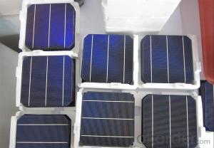
Usage and Applications of Poly Wafers
Poly Solar Wafers mainly used in Poly Solar Cells, with high efficiency and reliable quality. Our Wafer can promise the 25 years life span and have passed PID test.
Packaging & Delivery of Poly Wafers
Carton Box Package and Deliver by air
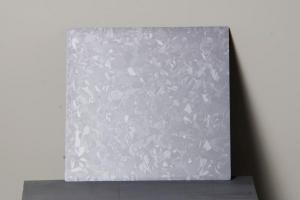
Factory Picture of Poly Wafers

Package Picture of Poly Wafers

- Q: Are there any initiatives to reduce the environmental impact of solar silicon wafer production?
- Yes, there are various initiatives aimed at reducing the environmental impact of solar silicon wafer production. These include the development and adoption of more sustainable manufacturing processes, such as the use of renewable energy sources in production facilities, reducing water usage, and implementing recycling programs for waste materials. Additionally, research is being conducted to explore alternative materials and techniques that could further minimize the environmental footprint of solar silicon wafer production.
- Q: Can solar silicon wafers be used in harsh climates?
- Yes, solar silicon wafers can be used in harsh climates. They are designed to withstand extreme weather conditions, including high temperatures, humidity, and even freezing temperatures. Additionally, they are often made with protective coatings to ensure durability and longevity in harsh environments.
- Q: Do solar silicon wafers emit any pollutants or greenhouse gases during operation?
- No, solar silicon wafers do not emit any pollutants or greenhouse gases during operation. Solar panels convert sunlight into electricity through a clean and renewable process, which does not involve any emissions or harmful byproducts.
- Q: Can solar silicon wafers be used in concentrated photovoltaic systems?
- Yes, solar silicon wafers can be used in concentrated photovoltaic systems. These systems use lenses or mirrors to concentrate sunlight onto smaller, more efficient solar cells, including silicon wafers. The concentration increases the amount of sunlight reaching the cells, resulting in higher energy output.
- Q: What is the meaning of a cleaning in a semiconductor silicon wafer process? RCA?
- () SPM:H2SO4 /H2O2 120 to 150 DEG C SPM has a high oxidation capacity, can be dissolved in the metal oxidation solution, and the oxidation of organic matter to generate CO 2 and H2O. The use of SPM to clean silicon wafers can remove heavy organic contaminants and some metals on the surface of silicon wafer, but it is difficult to remove organic matter when organic matter is particularly serious.
- Q: Can solar silicon wafers be used in agricultural applications?
- Yes, solar silicon wafers can be used in certain agricultural applications. They can be integrated into solar panels to power irrigation systems, electric fences, and other farm equipment. Additionally, solar-powered sensors and monitoring systems can be developed using silicon wafers to optimize crop growth and monitor environmental conditions in agricultural settings.
- Q: I grew up in the silicon chip Ag particles, the size of about a few hundred nanometers, I would like to ask how I do before the TEM sample?
- Finish drying, look at the actual situation on the electronic microscope. If the results can not be adjusted according to the situation of sample preparation.
- Q: Are there any limitations to the use of solar silicon wafers?
- Yes, there are limitations to the use of solar silicon wafers. One limitation is that they are relatively expensive to produce compared to other types of solar cells. Additionally, the efficiency of solar silicon wafer-based cells can decrease in high temperatures, leading to a decrease in overall performance. Another limitation is their brittle nature, making them prone to breakage during handling and transportation. Finally, the production process for silicon wafers involves the use of hazardous chemicals, which raises environmental concerns.
- Q: After wafer cleaning, how to change the film?
- 2, surface metal cleaning(1) HPM (SC22) cleaning (2) DHF cleaningMetal contamination of silicon surface has two kinds of adsorption and desorption mechanism: (1) compared with the negatively charged silicon high metal such as Cu, Ag, Au, from the silicon surface to capture electron on the surface of the silicon direct formation of chemical bonds. Has a high redox potential of the solution to obtain electrons from these metals, resulting in metal the ionized form dissolved in the solution, so that this type of metal removed from the silicon surface. (2) compared with the negatively charged silicon low metal, such as Fe, Ni, Cr, Al, Ca, Na, K can be easily ionized in solution and deposited on the silicon wafer surface natural oxide film or a chemical oxide film on these metals in dilute HF solution with a natural oxide film or a chemical oxide film is easily removed.3, organic cleaningThe removal of organic silicon surface cleaning fluid used is SPM.SPM with high oxidative capacity, metal oxide can be dissolved in solution, and the oxidation of organic compounds to produce CO2 and.SPM cleaning water can remove the surface of silicon wafer heavy organic contamination and some metal, but when organic contamination is heavy will make carbonization of organic matter and difficult to remove by SPM. After cleaning, the silicon surface residual sulfide, the sulfide particles is difficult to use to water wash out.
- Q: How are solar silicon wafers protected from thermal damage?
- Solar silicon wafers are protected from thermal damage through various methods. One common technique is the use of passivation layers, such as silicon nitride or silicon oxide, which act as a protective coating to prevent heat-induced degradation. These layers help to reduce surface recombination and enhance the overall efficiency of the solar cell. Additionally, the wafers may be encapsulated within a transparent and heat-resistant material, such as glass or polymer, which provides insulation and safeguards against thermal stress. Careful design and engineering of the solar cell structure also contribute to efficient heat dissipation, ensuring that the wafers can withstand high temperatures without sustaining damage.
Our company is a world class resources and green energy developer, operator and supplier with its engagement in green energy development, integration and operation. We strives to offer highly efficient, eco-friendly, economical and reliable energy solutions through an integrated and diversified energy industrial chain. In adherence to the philosophy of bringing green power to life, the Group stays committed to continuously providing high-quality energy and services for a better living environment. Under approaches of people-oriented, excellence-foremost, value-creation and harmony-pursuant, our Group is determined to become a respected world-class green energy conglomerate.
1. Manufacturer Overview
| Location | |
| Year Established | |
| Annual Output Value | |
| Main Markets | |
| Company Certifications |
2. Manufacturer Certificates
| a) Certification Name | |
| Range | |
| Reference | |
| Validity Period |
3. Manufacturer Capability
| a) Trade Capacity | |
| Nearest Port | |
| Export Percentage | |
| No.of Employees in Trade Department | |
| Language Spoken: | |
| b) Factory Information | |
| Factory Size: | |
| No. of Production Lines | |
| Contract Manufacturing | |
| Product Price Range | |
Send your message to us
Silicon Wafer in Solar Photovoltaic Cells - Polycrystalline/Multiple Solar Silicon Wafer 156*156
- Ref Price:
-
- Loading Port:
- Shanghai Port
- Payment Terms:
- TT or LC
- Min Order Qty:
- 100 Pieces PCS
- Supply Capability:
- 700MW/Per Year PCS/month
OKorder Service Pledge
Quality Product, Order Online Tracking, Timely Delivery
OKorder Financial Service
Credit Rating, Credit Services, Credit Purchasing
Similar products


Hot products


Hot Searches

