


Silicon Wafer Solar Cell - High Quality A Grade Mono Crystalline 5V 18.8%
- Ref Price:
-

- Loading Port:
- Shanghai
- Payment Terms:
- TT OR LC
- Min Order Qty:
- 1000 pc
- Supply Capability:
- 100000 pc/month
OKorder Service Pledge
OKorder Financial Service
You Might Also Like


Specifications
hot sale solar cell
1.16.8%~18.25% high efficiency
2.100% checked quality
3.ISO9001/ISO14001/TUV/CE/UL
4.stable performance
We can offer you the best quality products and services, don't miss !
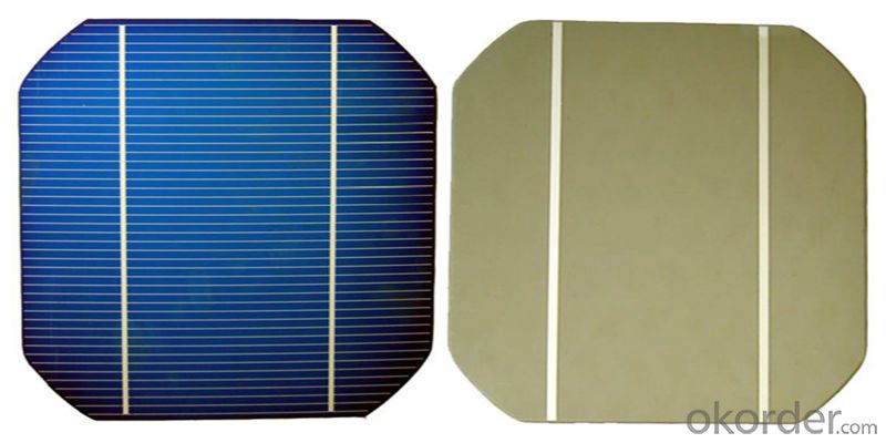
POLY6'(156*156)
Polycrystalline Silicon Solar cell
Physical Characteristics
Dimension: 156mm×156mm±0.5mm
Diagonal: 220mm±0.5mm
Thickness(Si): 200±20 μm
Front(-) Back(+)
Blue anti-reflecting coating (silicon nitride); Aluminum back surface field;
1.5mm wide bus bars; 2.0mm wide soldering pads;
Distance between bus bars: 51mm . Distance between bus bars :51mm .
Electrical Characteristics
Efficiency(%) | 18.00 | 17.80 | 17.60 | 17.40 | 17.20 | 16.80 | 16.60 | 16.40 | 16.20 | 16.00 | 15.80 | 15.60 |
Pmpp(W) | 4.33 | 4.29 | 4.24 | 4.19 | 4.14 | 4.09 | 4.04 | 3.99 | 3.94 | 3.90 | 3.86 | 3.82 |
Umpp(V) | 0.530 | 0.527 | 0.524 | 0.521 | 0.518 | 0.516 | 0.514 | 0.511 | 0.509 | 0.506 | 0.503 | 0.501 |
Impp(A) | 8.159 | 8.126 | 8.081 | 8.035 | 7.990 | 7.938 | 7.876 | 7.813 | 7.754 | 7.698 | 7.642 | 7.586 |
Uoc(V) | 0.633 | 0.631 | 0.628 | 0.625 | 0.623 | 0.620 | 0.618 | 0.617 | 0.615 | 0.613 | 0.611 | 0.609 |
Isc(A) | 8.709 | 8.677 | 8.629 | 8.578 | 8.531 | 8.478 | 8.419 | 8.356 | 8.289 | 8.220 | 8.151 | 8.083 |

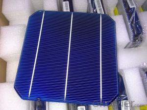
MONO5'(125*125mm)165
Monocrystalline silicon solar cell
Physical Characteristics
Dimension: 125mm×125mm±0.5mm
Diagonal: 165mm±0.5mm
Thickness(Si): 200±20 μm
Front(-) Back(+)
Blue anti-reflecting coating(silicon nitride); Aluminum back surface field;
1.6mmwide bus bars; 2.5mm wide soldering pads;
Distance between bus bars: 61mm . Distance between bus bars :61mm .
Electrical Characteristics
Efficiency(%) | 19.40 | 19.20 | 19.00 | 18.80 | 18.60 | 18.40 | 18.20 | 18.00 | 17.80 | 17.60 | 17.40 | 17.20 |
Pmpp(W) | 2.97 | 2.94 | 2.91 | 2.88 | 2.85 | 2.82 | 2.79 | 2.76 | 2.73 | 2.70 | 2.67 | 2.62 |
Umpp(V) | 0.537 | 0.535 | 0.533 | 0.531 | 0.527 | 0.524 | 0.521 | 0.518 | 0.516 | 0.515 | 0.513 | 0.509 |
Impp(A) | 5.531 | 5.495 | 5.460 | 5.424 | 5.408 | 5.382 | 5.355 | 5.328 | 5.291 | 5.243 | 5.195 | 4.147 |
Uoc(V) | 0.637 | 0.637 | 0.636 | 0.635 | 0.633 | 0.630 | 0.629 | 0.629 | 0.628 | 0.626 | 0.626 | 0.625 |
Isc(A) | 5.888 | 5.876 | 5.862 | 5.848 | 5.839 | 5.826 | 5.809 | 5.791 | 5.779 | 5.756 | 5.293 | 5.144 |

FAQ:
Q:How can i get some sample?
A:Yes , if you want order ,sample is not a problem.
Q:How about your solar panel efficency?
A: Our product efficency around 17.25%~18.25%.
Q:What’s the certificate you have got?
A: we have overall product certificate of ISO9001/ISO14001/CE/TUV/UL
- Q: What are the different surface texturing techniques used for solar silicon wafers?
- There are several surface texturing techniques used for solar silicon wafers, including chemical etching, plasma etching, laser texturing, and texturing through lithography. These techniques are employed to create a textured surface on the silicon wafer, which enhances light trapping and increases the efficiency of solar cells.
- Q: What is the expected efficiency improvement for bifacial solar silicon wafers?
- The expected efficiency improvement for bifacial solar silicon wafers varies depending on several factors such as the design of the module, installation conditions, and the overall system setup. However, studies have shown that bifacial solar silicon wafers can provide an efficiency improvement of around 10% to 30% compared to traditional monofacial solar panels.
- Q: What is the role of surface passivation in solar silicon wafers?
- The role of surface passivation in solar silicon wafers is to reduce or eliminate surface recombination, which is the process by which charge carriers (electrons and holes) recombine at the surface of the wafer, leading to a loss of efficiency in solar cell performance. Passivation involves applying a thin layer of material, such as silicon nitride or aluminum oxide, to the surface of the wafer to create a barrier that prevents the recombination of charge carriers. This helps to improve the efficiency and overall performance of the solar cell by reducing the loss of generated electricity due to surface recombination.
- Q: What is the market size for solar silicon wafers?
- The market size for solar silicon wafers is constantly evolving and expanding due to the growing demand for solar energy. As of 2021, it is estimated to be in the range of several billion dollars, with projections of further growth in the coming years.
- Q: What is the meaning of the wafer (100), the crystal orientation index or the crystal plane index?Also (1100 and (111) which direction and angle should be cut?
- The coordinate system is set up in the crystal cellIs the coordinate of the direction vector
- Q: What is the cost of a solar silicon wafer?
- The cost of a solar silicon wafer can vary depending on various factors such as the size, quality, and quantity ordered. On average, a standard 156 mm x 156 mm solar silicon wafer can cost around $0.20 to $0.50 per piece. However, it's important to note that prices may fluctuate due to market conditions and other factors.
- Q: Can solar silicon wafers be used in floating solar power plants?
- Yes, solar silicon wafers can be used in floating solar power plants. These wafers are often used in traditional solar panels and can also be applied to floating platforms. Floating solar power plants utilize these wafers to convert sunlight into electricity, just like land-based solar power plants. This allows for the generation of renewable energy in bodies of water, making floating solar power plants a viable option for maximizing solar energy production.
- Q: What is the purpose of an anti-reflective coating on a solar silicon wafer?
- The purpose of an anti-reflective coating on a solar silicon wafer is to minimize the amount of light that is reflected off the surface of the wafer. By reducing reflection, more light can be absorbed by the solar cells, resulting in increased efficiency and energy production.
- Q: How does the efficiency of a solar silicon wafer change with snow cover?
- The efficiency of a solar silicon wafer generally decreases with snow cover. The snow layer acts as an insulator, preventing sunlight from reaching the wafer and reducing the amount of energy that can be converted into electricity. Additionally, the presence of snow can cause shading and reflection, further reducing the efficiency of the solar panel.
- Q: What is the typical cost per watt for a solar silicon wafer?
- The typical cost per watt for a solar silicon wafer can vary depending on various factors such as the size and quality of the wafer, manufacturing processes, and market conditions. However, as of current estimations, the average cost per watt for a solar silicon wafer ranges between $0.20 to $0.30.
Send your message to us
Silicon Wafer Solar Cell - High Quality A Grade Mono Crystalline 5V 18.8%
- Ref Price:
-
- Loading Port:
- Shanghai
- Payment Terms:
- TT OR LC
- Min Order Qty:
- 1000 pc
- Supply Capability:
- 100000 pc/month
OKorder Service Pledge
OKorder Financial Service
Similar products


Hot products


Hot Searches
Related keywords

