

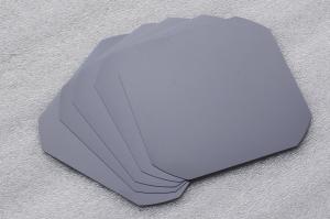


Solar Silicon Wafer - Monocrystalline Grade
- Ref Price:
-

- Loading Port:
- Shanghai Port
- Payment Terms:
- TT or LC
- Min Order Qty:
- 100Pieces PCS
- Supply Capability:
- 700 MW/Per Year PCS/month
OKorder Service Pledge
OKorder Financial Service
You Might Also Like


Specification of Mono Silicon Wafers
We can provide you solar wafer both156*156 and 125*125mm, Mono and Poly
Solar Wafers for your raw materials choice.
| Product name | Mono Wafer |
| Conductive type | P type |
| Square size wafer(mm) | 156×156±0.5 |
| Resistivity range | 1~3 ohm |
| Corner(mm) | 150±0.5;165±0.5 |
| 195±0.5;200±0.5 | |
| Thickness (μm) | 200±20 |
| Total thickness(um) | ≤ 30 |
| Resistivity range(Ωcm) | 1-3 |
| Doping elements | Boron |
| Orientation | (100)±1° |
| Carbon content(atoms/cc) | ≤1.0E+17 |
| Oxygen content(atoms/cc) | ≤1.0E+18 |
| Lifetime(μs) | ≥10 |
| Surface quality | No crack, gap, missing Angle, perforated, silicon fell and stress |
| Warping degrees(warp/μm) | ≤50 |
| Neighbouring vertical degree | 90±0.5° |
| Side damage(mm) | ≤0.5mm(length)×0.3mm(width)(not more than 2 per wafer) |
| Line mark(μm) | ≤15 |
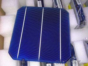
Usage and Applications of Mono Solar Wafers
Mono Solar Wafers mainly used in Solar Cells with reliable quality and trustful efficiency performance. Our Wafers should be your best choice for raw materials.
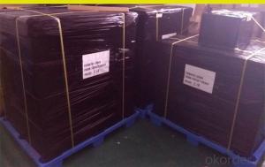
Packaging & Delivery of Mono Solar Wafers
Carton Box Package and Deliver by air. It should be avoid of moist, water and shaking to protect the safety of Solar Cells.
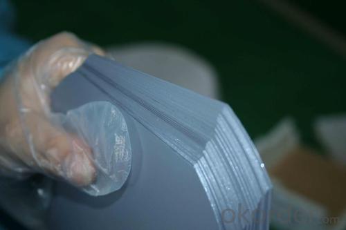
Factory Picture of Mono Solar Wafers

Package Picture of Mono Solar Wafers

- Q: How are solar silicon wafers handled and transported?
- Solar silicon wafers are handled and transported with great care to ensure their quality and integrity. They are typically stored in cleanroom environments to prevent contamination. When being transported, they are usually packaged in protective materials such as antistatic bags or foam inserts to prevent any damage or breakage. Specialized carriers or trucks equipped with shock-absorbing systems are used to minimize vibrations and impacts during transportation. Additionally, temperature and humidity control measures are implemented to avoid any adverse effects on the wafers. Overall, meticulous handling and secure packaging are essential to maintain the high quality of solar silicon wafers throughout their transportation process.
- Q: What are the different wafer orientations used in solar silicon wafer production?
- There are three main wafer orientations used in solar silicon wafer production: <100>, <111>, and <110>. The <100> orientation is the most commonly used, as it provides a balance between cost, efficiency, and ease of production. The <111> orientation is known for its high efficiency, but it is less commonly used due to its higher cost and more complex manufacturing process. The <110> orientation is used in specific applications where superior mechanical strength is required. Overall, the choice of wafer orientation depends on the desired balance between cost, efficiency, and specific application requirements.
- Q: How do solar silicon wafers contribute to the decentralization of energy production?
- Solar silicon wafers contribute to the decentralization of energy production by enabling the generation of electricity at the point of consumption. By converting sunlight into electricity, solar silicon wafers allow households, businesses, and even communities to produce their own energy on-site, reducing reliance on centralized power plants and grid infrastructure. This decentralization promotes energy independence, increases resilience, and reduces transmission losses, while also facilitating a shift towards cleaner and renewable sources of energy.
- Q: After cutting a few chips, mortar density is getting lower and lower
- There are a lot of things that could happen1 lubricant is not qualified2 too many bubbles in the recycle bin3 mortar selection4, the operation speed is too fast5 wafer density is not uniform (the lowest possible)Try not to contact
- Q: Polished silicon wafers can be most SEM substrates
- In other words, only nano materials will consider the use of polished silicon wafer sample carrier. Micron submicron level, waste, direct double-sided conductive adhesive tape can be.
- Q: Can solar silicon wafers be used in water pumping systems?
- Yes, solar silicon wafers can be used in water pumping systems. Solar silicon wafers are commonly used in photovoltaic (PV) cells to convert sunlight into electricity. This electricity can power the water pumping systems, making them more sustainable and environmentally friendly.
- Q: Can solar silicon wafers be used in solar-powered satellites?
- Yes, solar silicon wafers can indeed be used in solar-powered satellites. These wafers are commonly used in the manufacturing of solar cells, which are essential components of solar panels. Solar cells convert sunlight into electricity, making them ideal for powering satellites in space where solar energy is abundant.
- Q: What is the expected efficiency improvement for tandem quantum dot-silicon solar silicon wafers?
- The expected efficiency improvement for tandem quantum dot-silicon solar silicon wafers is quite significant. Tandem solar cells combine multiple layers of different materials to absorb a broader spectrum of sunlight and convert it into electricity more effectively. By integrating quantum dots with silicon wafers, which are already widely used in solar cell technology, the overall efficiency of the solar cells can be substantially increased. Although specific figures may vary depending on the design and implementation, tandem quantum dot-silicon solar silicon wafers have the potential to achieve efficiency improvements of 30% or more compared to traditional silicon solar cells.
- Q: How do solar silicon wafers perform in urban environments?
- Solar silicon wafers perform well in urban environments as they can efficiently generate electricity even in the presence of indirect or diffused sunlight. Their high conversion efficiency and ability to withstand various weather conditions make them a suitable choice for harnessing solar energy in cities. Moreover, advancements in technology have led to the development of more durable and efficient solar panels, further enhancing their performance in urban settings.
- Q: What are the aspects of silicon wafer testing?
- Silicon chips have side length 125mm, 156mm, and 125 of the large chamfer diagonal 156mm and small chamfer diagonal 165mm, polycrystalline silicon chip to the side of the 156mm based, diagonal 219.2mm.
1. Manufacturer Overview
| Location | |
| Year Established | |
| Annual Output Value | |
| Main Markets | |
| Company Certifications |
2. Manufacturer Certificates
| a) Certification Name | |
| Range | |
| Reference | |
| Validity Period |
3. Manufacturer Capability
| a) Trade Capacity | |
| Nearest Port | |
| Export Percentage | |
| No.of Employees in Trade Department | |
| Language Spoken: | |
| b) Factory Information | |
| Factory Size: | |
| No. of Production Lines | |
| Contract Manufacturing | |
| Product Price Range | |
Send your message to us
Solar Silicon Wafer - Monocrystalline Grade
- Ref Price:
-
- Loading Port:
- Shanghai Port
- Payment Terms:
- TT or LC
- Min Order Qty:
- 100Pieces PCS
- Supply Capability:
- 700 MW/Per Year PCS/month
OKorder Service Pledge
OKorder Financial Service
Similar products


Hot products


Hot Searches
Related keywords

