


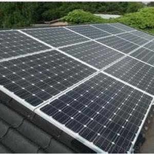
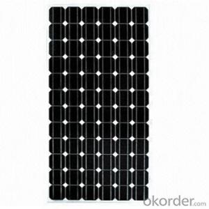
Power 185WP 6 Inch Monocrystaline Solar Panel
- Ref Price:
-

- Loading Port:
- China main port
- Payment Terms:
- TT OR LC
- Min Order Qty:
- 100 watt
- Supply Capability:
- 10000 watt/month
OKorder Service Pledge
OKorder Financial Service
You Might Also Like


Power 185WP 6" Poly Crystalline Solar Cell
Solar Module Summarize
Solar Module is the core part of solar PV power systems,also is the highest value part of it. The function of Solor Module is to convert the sun's radiation to electrical energy, or transfer it to battery and store in it, or to drive the load running.
The Product has been widely used in space and ground, it mainly used for power generation systems, charging systems, road lighting and traffic signs areas. It could offer a wide range of power and voltage, and with high conversion efficiency, and long service life.
Our Products
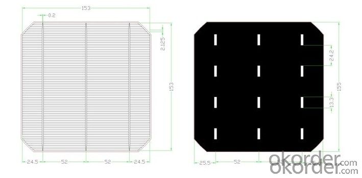
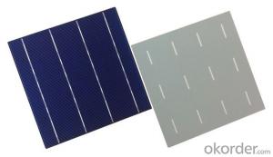
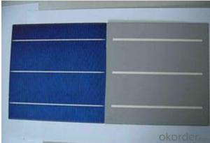
5x5 inch (125x125mm) mono solar cells and 6x6 inch (156x156mm) poly and mono solar cell
Mono-crystalline and Poly-crystalline solar panel from 3watt to 327watt
Home-use solar system 5W to 5KW
Other accessories like Inverter and battery etc.
Main Characteristic
Eff(%) | 18.00- 18.10 | 18.10- 18.20 | 18.20- 18.30 | 18.30- 18.40 | 18.40- 18.50 | 18.50- 18.60 | 18.60- 18.70 | 18.70- 18.80 | 18.80- 18.90 | 18.9- 19.0 | 19.1- 19.1 | 19.1- 19.2 |
Pm(W) | 4.30 | 4.33 | 4.35 | 4.37 | 4.40 | 4.42 | 4.44 | 4.47 | 4.49 | 4.52 | 4.54 | 4.56 |
Isc(A) | 8.71 | 8.73 | 8.76 | 8.77 | 8.78 | 8.82 | 8.83 | 8.85 | 8.86 | 8.88 | 8.9 | 8.93 |
Im(A) | 8.19 | 8.21 | 8.24 | 8.26 | 8.30 | 8.33 | 8.35 | 8.39 | 8.42 | 8.45 | 8.47 | 8.51 |
Voc(V) | 0.630 | 0.631 | 0.632 | 0.633 | 0.634 | 0.634 | 0.635 | 0.636 | 0.637 | 0.637 | 0.638 | 0.64 |
Vm(V) | 0.527 | 0.528 | 0.529 | 0.531 | 0.531 | 0.532 | 0.534 | 0.534 | 0.535 | 0.536 | 0.537 | 0.538 |
FF(%) | 78.6 | 78.7 | 78.8 | 79.0 | 79.2 | 79.3 | 79.5 | 79.6 | 79.8 | 80 | 80 | 80 |
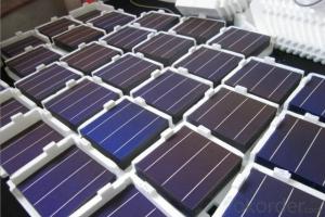
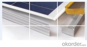
Product Show


Warranties
6Inch 2BB Polycrystalline Multi Solar Cells Mono Solar Cell
For c-Si panel: 25years output warranty for no less than 80% of performance, 10 years output warranty for no less than 90% of performance. Free from material and workmanship defects within 5 years.
For a-Si panel: 20 years output warranty for no less than 80% of performance, 10 years output warranty for no less than 90% of performance. Free from material and workmanship defects within 2 years.
- Q: How are solar silicon wafers interconnected to form solar modules?
- Solar silicon wafers are interconnected to form solar modules through a process called solar cell stringing. In this process, multiple silicon wafers are connected in series using metal conductive ribbons. The ribbons are soldered onto the front and back contacts of the adjacent wafers, creating an electrical pathway between them. This interconnection enables the flow of current generated by the individual solar cells, allowing them to work together efficiently and produce electricity.
- Q: Monocrystalline silicon processing technology
- The use of more than one set of cutting lines is an innovative way to increase the output of the machine under the condition of keeping the speed. The latest MaxEdge system of applied materials company uses a unique set of two independent control cutting components.MaxEdge is the industry's first use of specially designed fine wire secant system, the minimum can reach 80 M. Compared with the HCT B5 wire system applied materials industry leading, these improvements reduce the loss of the silicon material yield up to 50%.Wire system with higher productivity can reduce the number of tools in wafer yield under the same. Therefore, manufacturers can significantly reduce the cost of equipment, operators and maintenance.Reducing the consumption of silicon wafers is directly reducing the cost per watt of solar power.Wire products marketThe silicon wafer suppliers and hope to integrate the crystalline silicon PV module manufacturers to control their own slice process requires the use of wire saw device. Monocrystalline silicon and polycrystalline silicon photovoltaic technology are needed to use it.
- Q: What is the global production capacity of solar silicon wafers?
- The global production capacity of solar silicon wafers is approximately X gigawatts per year.
- Q: Wafer cutting will appear thick sheet, I would like to ask what the reasons are
- Solving measures:A. guide slot check slot is uniform, and to compensate for the loss according to the situation of the slot wheel.When the A. is set to zero, the position of the guide line is controlled.B. standard viscose operation. When the surface of the silicon block is bonded with the guide bar, the utility model can be used to check whether the guide strip is bent, and whether the glue is evenly applied, so that there is no gap between the guide strip and the silicon block after the bonding guide strip is arranged.In the process of using the C. guide wheel, the utility model is used to detect the guide groove of the guide wheel on a regular basis, and the depth and the angle of the guide groove are observed.
- Q: What is the role of surface passivation in solar silicon wafers?
- The role of surface passivation in solar silicon wafers is to reduce or eliminate surface recombination, which is the process by which charge carriers (electrons and holes) recombine at the surface of the wafer, leading to a loss of efficiency in solar cell performance. Passivation involves applying a thin layer of material, such as silicon nitride or aluminum oxide, to the surface of the wafer to create a barrier that prevents the recombination of charge carriers. This helps to improve the efficiency and overall performance of the solar cell by reducing the loss of generated electricity due to surface recombination.
- Q: 8 inch monocrystalline silicon area?
- Generally refers to the round wafer, 8 inch refers to the diameter of 8 inches, "=2.54cm", the area of the circle you will ask for 1.
- Q: Are solar silicon wafers affected by voltage surges?
- Yes, solar silicon wafers can be affected by voltage surges. Voltage surges can cause damage to the electronic components of solar panels, including the silicon wafers. It is important to have proper surge protection measures in place to mitigate the risk of damage from voltage surges.
- Q: What are the different doping techniques used in solar silicon wafers?
- There are several doping techniques used in solar silicon wafers, including diffusion, ion implantation, and screen-printing. Diffusion involves introducing dopant atoms, such as phosphorus or boron, into the silicon wafer by heating it in the presence of a dopant source. Ion implantation involves bombarding the wafer with dopant ions, which then become embedded in the silicon lattice. Screen-printing involves applying a dopant paste onto the surface of the wafer and then firing it to create a doped layer. These techniques are used to create the necessary p-n junctions and optimize the electrical properties of the solar cells.
- Q: Can solar silicon wafers be used in other applications besides solar panels?
- Yes, solar silicon wafers can be used in various other applications besides solar panels. They are commonly used in electronics, such as integrated circuits and microchips, due to their excellent electrical conductivity and thermal properties. Additionally, they can be utilized in the production of sensors, optoelectronics, and even in certain medical devices. The versatility and reliability of solar silicon wafers make them suitable for a range of applications beyond solar panels.
- Q: Can solar silicon wafers be used in tandem solar cell configurations?
- Yes, solar silicon wafers can be used in tandem solar cell configurations. Tandem solar cells are constructed by stacking multiple solar cell layers, each with a different bandgap, to achieve higher efficiency. Silicon wafers are commonly used in the bottom cell of tandem configurations due to their cost-effectiveness and compatibility with other materials.
Send your message to us
Power 185WP 6 Inch Monocrystaline Solar Panel
- Ref Price:
-
- Loading Port:
- China main port
- Payment Terms:
- TT OR LC
- Min Order Qty:
- 100 watt
- Supply Capability:
- 10000 watt/month
OKorder Service Pledge
OKorder Financial Service
Similar products

Hot products


Hot Searches
Related keywords

