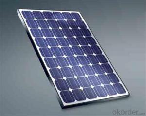
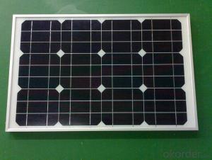


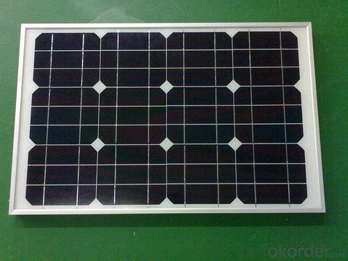


240w Mono Silicon Solar Wafer Panels for Home Use Solar Power System
- Ref Price:
-

- Loading Port:
- China main port
- Payment Terms:
- TT OR LC
- Min Order Qty:
- 10000 watt
- Supply Capability:
- 20000000 watt/month
OKorder Service Pledge
OKorder Financial Service
You Might Also Like


Destription:
Solar panel refers to a panel designed to absorb the sun's rays as a source of energy for generating electricity or heating. A PV module is a packaged, connected assembly of typically 6×10 solar cells. Solar PV panels constitute the solar array of a photovoltaic system that generates and supplies solar electricity in commercial and residential applications.
Main Characteristic
1.Manufactured according to international quality and Environment Management
System (ISO9001, ISO14001)
2. By the high transmittance, low iron tempered glass, anti-aging of the EVA(polyethylene - vinyl acetate), high-performance crystalline silicon solar cells, good Weather resistance TPT (fluoroplastics composite membrane) by pyramid , has a good Weather resistance and anti-UV, hail, water-proof capacity.
3. OEM and customerized package are accepted
4. High efficiency crystalline silicon solar cells
Quality warranty
1.10 years limited warranty on material and workmanship
2. more than 90% power output in 10 years
3. more than 80% power output in 25 years
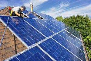
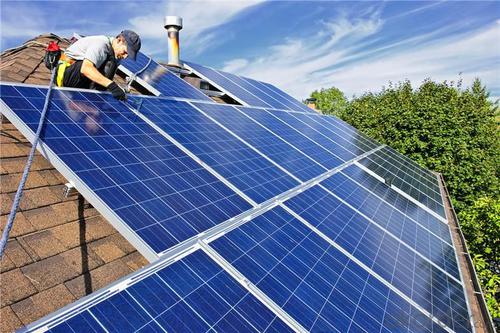
Product show


- Q: What is the role of antireflection coatings on solar silicon wafers?
- The role of antireflection coatings on solar silicon wafers is to reduce the amount of light reflection and increase the amount of light absorption by the solar cells. These coatings are designed to minimize the loss of solar energy caused by surface reflections, allowing more sunlight to penetrate the silicon wafer and convert into electricity. By enhancing light transmission, antireflection coatings improve the overall efficiency and performance of solar panels.
- Q: What is the typical efficiency degradation rate of a solar silicon wafer over time?
- The typical efficiency degradation rate of a solar silicon wafer over time is around 0.5-0.8% per year.
- Q: What is the role of surface passivation layers on solar silicon wafers?
- The role of surface passivation layers on solar silicon wafers is to minimize surface recombination, which significantly improves the efficiency of solar cells. These layers act as a barrier, preventing the loss of charge carriers and reducing the chances of electron-hole pairs recombining at the surface. By passivating the surface, these layers help to enhance the electrical properties of the solar cell, allowing for better absorption and conversion of sunlight into electricity.
- Q: What is a silicon wafer
- Silicon is an important material in the IC fabrication, through photolithography and ion implantation on the silicon wafer and other means, can be made into various semiconductor devices made of silicon chip. With amazing computational capabilities. The development of science and technology promotes the development of semiconductor. Development of automation and computer technology, this makes the silicon chip (integrated circuit) high technology product cost has been reduced to a very low degree. This makes the silicon wafer has been widely used in aerospace, industry, agriculture and national defense, and even crept into every family.
- Q: How to convert photovoltaic silicon MW
- 156 single crystal (chamfer 200) area: 238.95125 single crystal (chamfer 165) area: 154.831MW=1 * (10 negative) W
- Q: What is the impact of impurities on the reliability of solar silicon wafers?
- The presence of impurities in solar silicon wafers can significantly impact their reliability. Impurities can affect the electrical properties of the wafer, leading to decreased efficiency and performance of the solar cells. They can cause non-uniformity in the material, resulting in variations in cell performance within a module or across different modules. Moreover, impurities can also induce defects and degradation mechanisms that can reduce the lifespan of the solar cells. Therefore, minimizing impurities during the manufacturing process is crucial for ensuring the long-term reliability and efficiency of solar silicon wafers.
- Q: How does the efficiency of a solar silicon wafer vary with different light conditions?
- The efficiency of a solar silicon wafer varies with different light conditions. In general, the efficiency tends to increase with higher light intensity and direct sunlight. However, factors such as the angle of incidence, temperature, and wavelength of the light can also influence the efficiency.
- Q: What is the typical lifetime energy yield of a solar silicon wafer?
- The typical lifetime energy yield of a solar silicon wafer varies depending on various factors such as the efficiency of the solar cells, the geographical location, and the maintenance of the solar panel system. On average, a solar silicon wafer can generate enough energy to offset its initial embodied energy within 1-4 years. Over its lifetime, a solar silicon wafer can produce around 10-20 times more energy than was used in its manufacturing process.
- Q: What are the different types of solar silicon wafers?
- There are mainly three types of solar silicon wafers: monocrystalline, polycrystalline, and amorphous. Monocrystalline wafers are made from a single crystal structure and are known for their high efficiency. Polycrystalline wafers are made from multiple crystals and are less expensive but slightly less efficient. Amorphous wafers are non-crystalline and have the lowest efficiency, but they are flexible and can be used in flexible solar panels.
- Q: How are defects in solar silicon wafers detected?
- Defects in solar silicon wafers are typically detected using various techniques such as visual inspection, infrared imaging, and electrical testing. Visual inspection involves examining the wafer's surface for visible imperfections, such as cracks, scratches, or impurities. Infrared imaging can identify defects by measuring the heat distribution across the wafer, as irregularities often generate different thermal patterns. Electrical testing is conducted by applying a voltage or current to the wafer and analyzing its response to identify any anomalies or abnormalities. These techniques allow manufacturers to identify and remove defective wafers, ensuring the production of high-quality solar cells.
Send your message to us
240w Mono Silicon Solar Wafer Panels for Home Use Solar Power System
- Ref Price:
-
- Loading Port:
- China main port
- Payment Terms:
- TT OR LC
- Min Order Qty:
- 10000 watt
- Supply Capability:
- 20000000 watt/month
OKorder Service Pledge
OKorder Financial Service
Similar products
Hot products


Hot Searches
Related keywords

