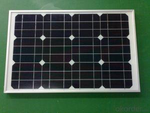


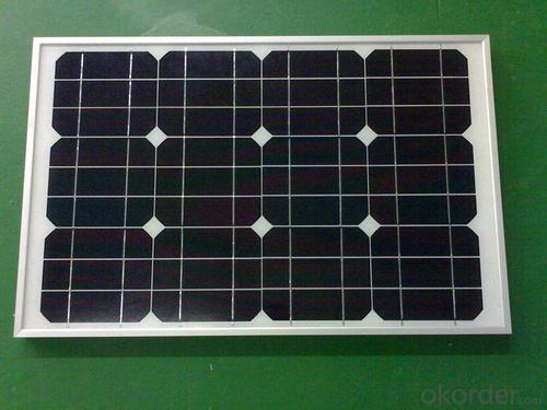

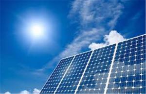
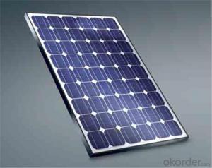
255w Silicone Wafer Solar Panels for Home Use Solar Power System
- Ref Price:
-

- Loading Port:
- China main port
- Payment Terms:
- TT OR LC
- Min Order Qty:
- 10000 watt
- Supply Capability:
- 20000000 watt/month
OKorder Service Pledge
OKorder Financial Service
You Might Also Like


Destription:
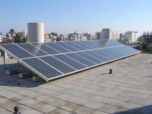
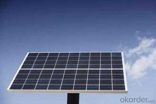
Solar panel refers to a panel designed to absorb the sun's rays as a source of energy for generating electricity or heating. A PV module is a packaged, connected assembly of typically 6×10 solar cells. Solar PV panels constitute the solar array of a photovoltaic system that generates and supplies solar electricity in commercial and residential applications.
Main Characteristic
1.Manufactured according to international quality and Environment Management
System (ISO9001, ISO14001)
2. By the high transmittance, low iron tempered glass, anti-aging of the EVA(polyethylene - vinyl acetate), high-performance crystalline silicon solar cells, good Weather resistance TPT (fluoroplastics composite membrane) by pyramid , has a good Weather resistance and anti-UV, hail, water-proof capacity.
3. OEM and customerized package are accepted
4. High efficiency crystalline silicon solar cells
Quality warranty
1.10 years limited warranty on material and workmanship
2. more than 90% power output in 10 years
3. more than 80% power output in 25 years
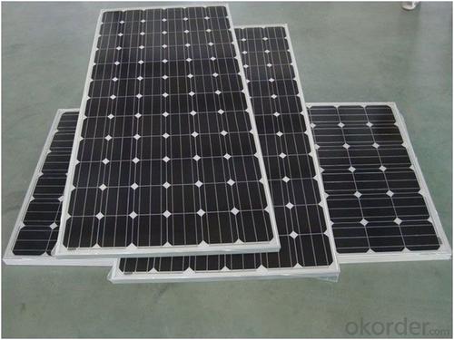
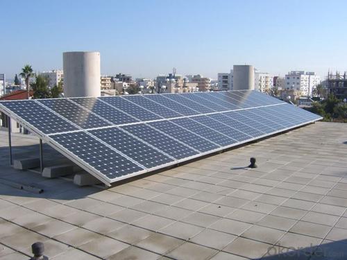
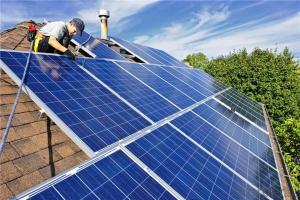
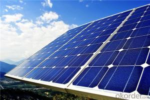
Product show


- Q: What is the role of back contacts on solar silicon wafers?
- The role of back contacts on solar silicon wafers is to provide an electrical connection between the silicon wafer and the external circuitry of the solar cell. They help in collecting the generated electricity from the front surface of the cell and ensure efficient transfer of the electrical current to the external load. Additionally, back contacts also help in providing structural support to the silicon wafer, allowing for easier handling and integration into the overall solar module.
- Q: How are solar silicon wafers used in solar panels?
- Solar silicon wafers are the building blocks of solar panels. They are made from highly purified silicon and are used to convert sunlight into electricity. These wafers are carefully arranged and connected to form solar cells, which then make up the solar panels. When sunlight hits the silicon wafer, the energy from the photons is absorbed, causing electrons to be released. These electrons are then captured and conducted through the solar panel, generating a flow of electricity. Ultimately, solar silicon wafers are essential components in harnessing solar energy for renewable power generation.
- Q: I work in a solar cell company, do silicon chip testing on the human body what chronic harm?
- Silicon is a semiconductor material, if it is to detect the bare silicon wafer, then there is no harm
- Q: Can solar silicon wafers be reused or repurposed after their lifespan in a solar panel?
- Yes, solar silicon wafers can be reused or repurposed after their lifespan in a solar panel. These wafers can undergo recycling processes to extract the valuable silicon material and then be used to manufacture new solar panels or other electronic components. Additionally, they can also be repurposed for various applications such as in the production of batteries or semiconductors, contributing to a more sustainable and circular economy.
- Q: How do solar silicon wafers perform in high-wind conditions?
- Solar silicon wafers are generally designed to withstand high-wind conditions. They are made from sturdy materials and undergo rigorous testing to ensure durability. Additionally, solar panels are typically mounted securely onto structures to minimize the impact of strong winds. While extremely powerful winds may cause some stress on the panels, proper installation and design measures help to ensure their performance and longevity even in high-wind conditions.
- Q: Can solar silicon wafers be used in building-integrated photovoltaics (BIPV)?
- Yes, solar silicon wafers can be used in building-integrated photovoltaics (BIPV). BIPV systems incorporate solar panels directly into building materials such as windows, roofs, or facades, allowing them to generate electricity while seamlessly blending into the building's architecture. Silicon wafers are commonly used in the production of solar cells, which can be integrated into various building components, making BIPV an efficient and aesthetically pleasing renewable energy solution.
- Q: Why integrated circuits are rectangular and the silicon chips are round
- Chip makers use a number of processes to integrate the integrated circuit on the circle. And an integrated circuit with more than a dozen or even hundreds of chips. After the completion of the results according to India to cut it, cut into small pieces of a small square. Then the small silicon chip is packaged with other materials and pins into an integrated circuit chip.
- Q: What is the production capacity of solar silicon wafers worldwide?
- The production capacity of solar silicon wafers worldwide is estimated to be in the range of tens of gigawatts (GW) per year.
- Q: How are solar silicon wafers protected from theft or unauthorized use?
- Solar silicon wafers are typically protected from theft or unauthorized use through several measures. These measures include physical security measures such as surveillance cameras, secure storage facilities, and restricted access to manufacturing facilities. Additionally, strict inventory management processes and tracking systems are implemented to ensure the traceability and accountability of each wafer. Furthermore, many manufacturers also employ advanced anti-counterfeiting techniques like unique identifiers or holograms on the wafers, making it difficult for unauthorized use or resale. Overall, a combination of physical security measures, strict inventory management, and anti-counterfeiting techniques help safeguard solar silicon wafers from theft or unauthorized use.
- Q: Specific kind of industry to use the reference price is what?!I have a ton of silicon chips, want to sell, do not know what the price, do not know what the company needs!
- List of productsPolycrystalline silicon ingot (Figure) silicon wafer (Figure)Battery (Figure) aluminum alloy color frame components (Figure)Epoxy resin encapsulation component photoelectric curtain wall component (all glass component)Solar lawn lamp (map) solar garden lamp (Figure)Solar communication power supply (map) solar mobile power supply (map)
Send your message to us
255w Silicone Wafer Solar Panels for Home Use Solar Power System
- Ref Price:
-
- Loading Port:
- China main port
- Payment Terms:
- TT OR LC
- Min Order Qty:
- 10000 watt
- Supply Capability:
- 20000000 watt/month
OKorder Service Pledge
OKorder Financial Service
Similar products
Hot products


Hot Searches
Related keywords

