


Ic Grade Solar Silicon Wafer 3kw Off-Grid Solar Energy Generator System for Home Solar Cell
- Ref Price:
-

- Loading Port:
- China main port
- Payment Terms:
- TT OR LC
- Min Order Qty:
- 100 watt
- Supply Capability:
- 10000 watt/month
OKorder Service Pledge
OKorder Financial Service
You Might Also Like


156x156 A Grade B Grade PV Silicon Solar Cell for Solar Panel
Solar Module Summarize
Solar Module is the core part of solar PV power systems,also is the highest value part of it. The function of Solor Module is to convert the sun's radiation to electrical energy, or transfer it to battery and store in it, or to drive the load running.
The Product has been widely used in space and ground, it mainly used for power generation systems, charging systems, road lighting and traffic signs areas. It could offer a wide range of power and voltage, and with high conversion efficiency, and long service life.
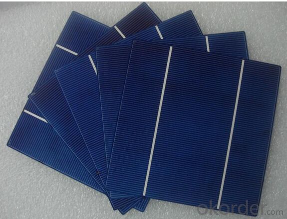
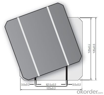
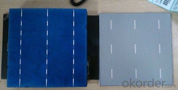
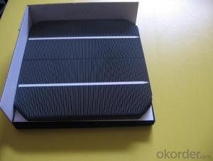
Physical characteristics
Dimension | 156mm X 156 mm ±0.5mm |
Wafer Thickness | 200um ±30um |
Front(-) | Four 1.1mm wide bus bars(silver) with distance 39mm, Acid texturized surface with blue silicon nitride AR coating. |
Back(+) | 2.4mm wide silver/aluminum soldering pads, aluminum back surface field. |
Product Pictures


- Q: Can solar silicon wafers be used in disaster response vehicles?
- Yes, solar silicon wafers can be used in disaster response vehicles. They can be used to harness solar energy and power various systems and equipment in these vehicles, providing a sustainable and reliable source of power during emergency situations.
- Q: What are the reasons for the emergence of the black chip phenomenon of the monocrystalline silicon, which aspects of the production process have an impact on it, preventive measures, and improvement measures?
- You say the phenomenon called flower piece, the formation of many factors, the main reason is that contamination, because in the process, the wafer surface after polishing the silicon atom is bond breaking, it is easy to adsorb metal ions and cannot completely by cleaning out.
- Q: How do solar silicon wafers contribute to job creation in the solar industry?
- Solar silicon wafers contribute to job creation in the solar industry by creating employment opportunities at various stages of the manufacturing process. The production of silicon wafers requires skilled workers to extract and refine the raw materials, operate the manufacturing equipment, and conduct quality control. Additionally, the installation and maintenance of solar panels, which utilize these wafers, create jobs for technicians and engineers in the solar industry. The growing demand for solar energy worldwide has led to the expansion of manufacturing facilities, thereby increasing job opportunities in the sector.
- Q: How do solar silicon wafers perform in areas with limited sunlight?
- Solar silicon wafers perform less efficiently in areas with limited sunlight compared to regions with abundant sunlight. The generation of electricity from solar panels is directly dependent on the amount of sunlight they receive. Therefore, in areas with limited sunlight, solar silicon wafers produce less electricity, resulting in reduced energy generation.
- Q: How is a backsheet attached to a solar silicon wafer?
- A backsheet is typically attached to a solar silicon wafer using a strong adhesive or encapsulant material. The backsheet is carefully positioned and secured onto the surface of the wafer, providing protection and insulation for the solar cells against environmental factors such as moisture, heat, and UV radiation.
- Q: Can solar silicon wafers be used in solar-powered electric fences?
- Yes, solar silicon wafers can be used in solar-powered electric fences. The wafers are used in solar panels to convert sunlight into electricity, which can then power the electric fence system.
- Q: How long do solar silicon wafers last in a solar panel?
- Solar silicon wafers can last for several decades in a solar panel, typically around 25 to 30 years.
- Q: What is the role of a glass cover in a solar silicon wafer?
- The role of a glass cover in a solar silicon wafer is to protect the wafer from external environmental factors such as dust, moisture, and mechanical damage. It provides a barrier that prevents the silicon wafer from getting scratched, contaminated, or oxidized, which could negatively impact its performance and efficiency. Additionally, the glass cover helps to optimize the transmission of sunlight onto the silicon wafer, enhancing the absorption of solar energy and maximizing the overall power output of the solar cell.
- Q: How is a grounding wire connected to a solar silicon wafer?
- A grounding wire is typically connected to a solar silicon wafer by attaching it to the metal frame or the backside of the wafer using a conductive adhesive or a soldering process.
- Q: What is the impact of crystal defects on the performance of solar silicon wafers?
- Crystal defects in solar silicon wafers can have a significant impact on their performance. These defects can include impurities, dislocations, and vacancies within the crystal lattice structure. These defects can reduce the efficiency of solar cells by affecting the flow of electrons and the generation of electric current. They can also lead to increased recombination of charge carriers, resulting in decreased power output and overall performance. Therefore, minimizing crystal defects is crucial in order to enhance the efficiency and performance of solar silicon wafers.
Send your message to us
Ic Grade Solar Silicon Wafer 3kw Off-Grid Solar Energy Generator System for Home Solar Cell
- Ref Price:
-
- Loading Port:
- China main port
- Payment Terms:
- TT OR LC
- Min Order Qty:
- 100 watt
- Supply Capability:
- 10000 watt/month
OKorder Service Pledge
OKorder Financial Service
Similar products


Hot products


Hot Searches
Related keywords

