


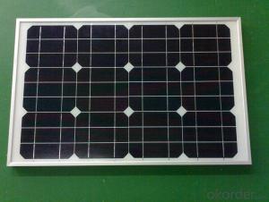
245w Wafer-Based Crystalline Silicon Solar Panels for Home Use Solar Power System
- Ref Price:
-

- Loading Port:
- China main port
- Payment Terms:
- TT OR LC
- Min Order Qty:
- 10000 watt
- Supply Capability:
- 20000000 watt/month
OKorder Service Pledge
OKorder Financial Service
You Might Also Like


Destription:
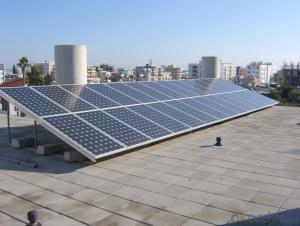
Solar panel refers to a panel designed to absorb the sun's rays as a source of energy for generating electricity or heating. A PV module is a packaged, connected assembly of typically 6×10 solar cells. Solar PV panels constitute the solar array of a photovoltaic system that generates and supplies solar electricity in commercial and residential applications.
Main Characteristic
1.Manufactured according to international quality and Environment Management
System (ISO9001, ISO14001)
2. By the high transmittance, low iron tempered glass, anti-aging of the EVA(polyethylene - vinyl acetate), high-performance crystalline silicon solar cells, good Weather resistance TPT (fluoroplastics composite membrane) by pyramid , has a good Weather resistance and anti-UV, hail, water-proof capacity.
3. OEM and customerized package are accepted
4. High efficiency crystalline silicon solar cells
Quality warranty
1.10 years limited warranty on material and workmanship
2. more than 90% power output in 10 years
3. more than 80% power output in 25 years
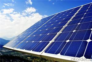
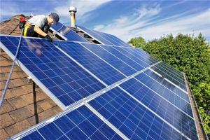
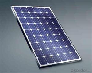
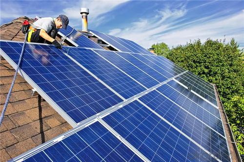
Product show


- Q: I would like to ask: silicon annealing treatment is how? Why anneal? Does annealing have an effect on the resistivity and the minority lifetime?
- Silicon wafer annealing process, is a part of the process. According to a certain procedure, the process of heating and cooling..;
- Q: What are the reasons for the emergence of the black chip phenomenon of the monocrystalline silicon, which aspects of the production process have an impact on it, preventive measures, and improvement measures?
- You say the phenomenon called flower piece, the formation of many factors, the main reason is that contamination, because in the process, the wafer surface after polishing the silicon atom is bond breaking, it is easy to adsorb metal ions and cannot completely by cleaning out.
- Q: What is the impact of wafer thickness on solar silicon wafer performance?
- The impact of wafer thickness on solar silicon wafer performance is significant. Thicker wafers tend to have higher mechanical strength and better resistance to cracking, making them more durable during handling and installation. However, thicker wafers also have higher light absorption, leading to increased optical losses and reduced overall efficiency. On the other hand, thinner wafers have lower light absorption losses but are more prone to breakage, especially during fabrication and handling processes. Therefore, finding an optimal balance between wafer thickness and performance is crucial for maximizing solar cell efficiency and ensuring cost-effectiveness in the solar industry.
- Q: Can solar silicon wafers be used in concentrated photovoltaic systems?
- Yes, solar silicon wafers can be used in concentrated photovoltaic systems. These systems use lenses or mirrors to concentrate sunlight onto smaller areas of solar cells, which can be made using silicon wafers. This concentration helps increase the efficiency of the photovoltaic system by focusing more sunlight onto the solar cells and generating more electricity.
- Q: What is the role of a power optimizer in a solar silicon wafer?
- The role of a power optimizer in a solar silicon wafer is to maximize the overall energy production and efficiency of the solar panel system. It achieves this by individually optimizing the performance of each solar module within the system, overcoming any shading, mismatch, or degradation issues. The power optimizer ensures that each solar module operates at its maximum power point, resulting in increased energy yield and improved system performance.
- Q: What is the impact of light-induced degradation on solar silicon wafers?
- Light-induced degradation, also known as LID, has a significant impact on solar silicon wafers. It causes a decrease in the efficiency and performance of the solar cells over time. LID occurs when the silicon material is exposed to light, particularly in the presence of boron or oxygen impurities. This exposure leads to the creation of defects and traps within the material, which results in a decrease in the solar cell's ability to generate electricity. Consequently, LID reduces the overall power output of the solar panel and requires additional measures to mitigate its effects, such as anti-LID coatings or improved cell designs.
- Q: What are the main challenges in manufacturing solar silicon wafers?
- The main challenges in manufacturing solar silicon wafers include high production costs, energy-intensive processes, and the need for high purity silicon. Additionally, the industry faces challenges in developing efficient methods for recycling and reducing waste during the manufacturing process.
- Q: Are there any safety concerns associated with handling solar silicon wafers?
- Yes, there are safety concerns associated with handling solar silicon wafers. Silicon wafers are fragile and can easily break, leading to potential lacerations or puncture injuries. Additionally, the wafers are often coated with various chemicals, such as photoresist or anti-reflective coatings, which may be hazardous if inhaled or ingested. It is essential to follow proper handling procedures, wear appropriate personal protective equipment, and work in a controlled environment to minimize any potential risks.
- Q: What is the role of solar silicon wafers in reducing air pollution?
- Solar silicon wafers play a crucial role in reducing air pollution by enabling the production of clean and renewable energy through solar panels. These wafers are made from purified silicon, which is a key component in photovoltaic cells. When sunlight hits the silicon wafer, it generates electricity without emitting harmful pollutants like greenhouse gases or particulate matter. By harnessing solar energy, we can reduce our reliance on fossil fuels and decrease air pollution from traditional power sources, ultimately contributing to a cleaner and healthier environment.
- Q: How is a solar silicon wafer connected to other components in a solar panel?
- A solar silicon wafer is typically connected to other components in a solar panel through a process called soldering. Soldering involves using a soldering iron to melt solder, a metal alloy, and then applying it to the connections between the wafer and other components. This creates a strong electrical and mechanical bond, allowing for efficient transfer of electricity within the solar panel.
Send your message to us
245w Wafer-Based Crystalline Silicon Solar Panels for Home Use Solar Power System
- Ref Price:
-
- Loading Port:
- China main port
- Payment Terms:
- TT OR LC
- Min Order Qty:
- 10000 watt
- Supply Capability:
- 20000000 watt/month
OKorder Service Pledge
OKorder Financial Service
Similar products

Hot products


Hot Searches
Related keywords

