


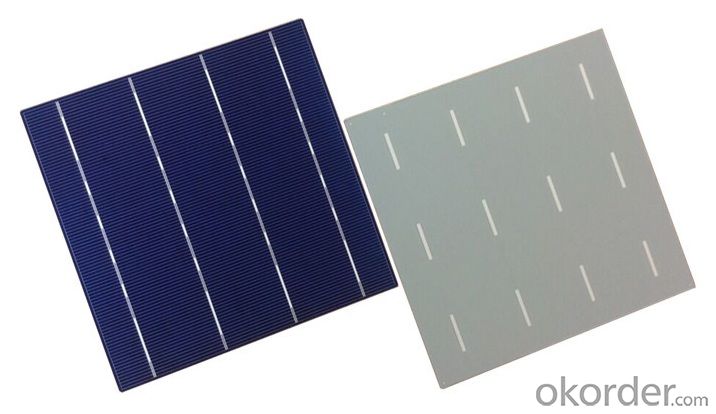

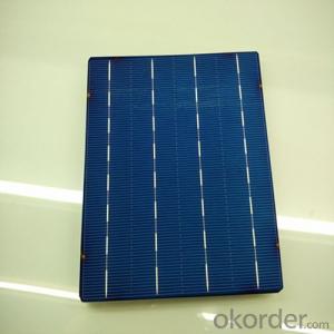
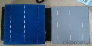
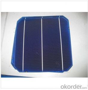
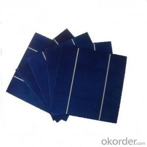
156*156mm 3BB Mono-crystalline Silicon Solar Cell
- Ref Price:
-

- Loading Port:
- China main port
- Payment Terms:
- TT OR LC
- Min Order Qty:
- 100 watt
- Supply Capability:
- 10000 watt/month
OKorder Service Pledge
OKorder Financial Service
You Might Also Like


156*156mm 3BB Mono-crystalline Silicon Solar Cell
Solar Module Summarize
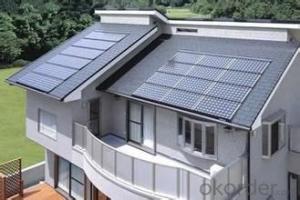
Solar Module is the core part of solar PV power systems,also is the highest value part of it. The function of Solor Module is to convert the sun's radiation to electrical energy, or transfer it to battery and store in it, or to drive the load running.
The Product has been widely used in space and ground, it mainly used for power generation systems, charging systems, road lighting and traffic signs areas. It could offer a wide range of power and voltage, and with high conversion efficiency, and long service life.
Dimension | 156mm X 156 mm ±0.5mm |
Wafer Thickness | 200um ±30um |
Front(-) | Four 1.1mm wide bus bars(silver) with distance 39mm, Acid texturized surface with blue silicon nitride AR coating. |
Back(+) | 2.4mm wide silver/aluminum soldering pads, aluminum back surface field. |
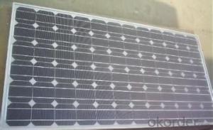
Product Show


Package
Typical package for one carton contains 1,200 cells. The cells are sealed in cell box every 100 pcs.
Gross weight per unit carton shall be around 16.4kg.
- Q: What is the effect of temperature on the efficiency of a solar silicon wafer?
- The temperature has a significant effect on the efficiency of a solar silicon wafer. As the temperature increases, the efficiency of the wafer decreases. This is because higher temperatures can lead to increased resistance in the wafer, which in turn reduces the flow of electricity. Additionally, higher temperatures can cause the semiconductor properties of the wafer to degrade, resulting in a decrease in its ability to convert sunlight into electricity. Therefore, controlling and minimizing the temperature of the solar silicon wafer is crucial for maximizing its efficiency and overall performance.
- Q: What is the role of passivation in solar silicon wafers?
- The role of passivation in solar silicon wafers is to improve the efficiency and performance of solar cells by reducing surface recombination and enhancing the charge carrier lifetime. Passivation helps to minimize the loss of electrons and holes at the surface of the wafer, allowing for better collection and utilization of light-generated carriers. This process involves applying a thin layer of passivating material, such as silicon nitride or aluminum oxide, to the surface of the wafer, which acts as a protective barrier and prevents the formation of traps and defects that can hinder the flow of charge carriers. Overall, passivation plays a crucial role in maximizing the conversion of sunlight into electricity in solar cells.
- Q: What is the role of solar silicon wafers in rural electrification?
- Solar silicon wafers play a crucial role in rural electrification by serving as the key component in solar photovoltaic panels. These wafers are responsible for converting sunlight into electricity, enabling the generation of clean and sustainable energy in remote rural areas. By harnessing solar power through the use of silicon wafers, rural communities gain access to reliable electricity, reducing their dependence on traditional and often unreliable sources such as diesel generators or kerosene lamps. This contributes to improving living conditions, promoting economic development, and reducing carbon emissions, ultimately supporting the goal of achieving universal energy access in rural areas.
- Q: How is a mounting structure attached to a solar silicon wafer?
- A mounting structure is typically attached to a solar silicon wafer using a conductive adhesive or soldering technique. The adhesive or solder is applied to the backside of the wafer, and the mounting structure is then pressed onto it. This ensures a secure and reliable connection between the wafer and the mounting structure, enabling the efficient installation and operation of the solar panel.
- Q: How are solar silicon wafers packaged and shipped?
- Solar silicon wafers are typically packaged and shipped in protective containers to ensure their safe transportation. These containers may include trays or boxes with foam inserts or anti-static materials to prevent any damage or contamination during transit. The packaged wafers are then usually stacked and secured on pallets or in crates for easier handling and transportation. Additionally, specific labeling and marking are applied to indicate the fragility and sensitivity of the wafers, ensuring careful handling throughout the shipping process.
- Q: Is solar silicon wafer often harmful to the body?
- . The main materials used in solar cells, such as single crystal silicon wafers, metal products, silver electrodes, etc., are harmless to the human body. Immature production process may lead to harmful gases such as dust, light and heat electromagnetic radiation, noise, etc..
- Q: How much energy is needed to produce a solar silicon wafer?
- The amount of energy required to produce a solar silicon wafer can vary depending on several factors such as the manufacturing process, technology used, and efficiency of the production facility. However, on average, it is estimated that around 250-350 kilowatt-hours (kWh) of energy are needed to manufacture one square meter of a standard silicon wafer for solar panels.
- Q: What is the price of monocrystalline silicon
- The content of silicon in the earth's crust is 25.8%, which provides an inexhaustible source for the production of monocrystalline silicon. Because silicon is one of the most abundant elements in the earth, the solar battery that destined to enter the mass market (mass market) products, reserves of advantage is to become one of the reasons the main photovoltaic silicon materials.
- Q: How are solar silicon wafers protected from lightning strikes?
- Solar silicon wafers are typically protected from lightning strikes through the implementation of lightning arresters and grounding systems. These systems divert the electrical energy from the lightning strike away from the wafers, ensuring their safety and preventing damage.
- Q: What is a silicon chip used for?What does it have to do with semiconductors.What are the components on the PCB board with silicon?
- But a good silicon chip is not available. Because the bare silicon wafer is not easy to damage and difficult to connect. This is a process of binding, the so-called binding is bound to use a very fine gold wire from the silicon chip lead wire, received on the metal pipe, and then use the non-conductive plastic to bind the chip sealed. We generally see transistors, chips, etc. are packaged, you simply can not see the inside of the core. Of course is also useful in metal or ceramic chip shell, such as the two or three level of some high power tubes, military grade components etc., but because the metal and ceramic package cost is relatively high, so most of the circuit or engineering plastic package.PCB is a printed circuit board, is what we call the board. The copper wire and the welding of various components and chips. The manufacturing of printed circuit board, you should check the information bar, then I talk today what also don't want to do
Send your message to us
156*156mm 3BB Mono-crystalline Silicon Solar Cell
- Ref Price:
-
- Loading Port:
- China main port
- Payment Terms:
- TT OR LC
- Min Order Qty:
- 100 watt
- Supply Capability:
- 10000 watt/month
OKorder Service Pledge
OKorder Financial Service
Similar products
Hot products


Hot Searches
Related keywords

