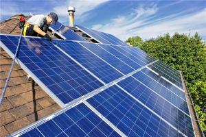
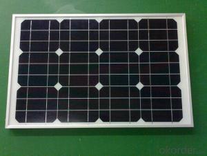

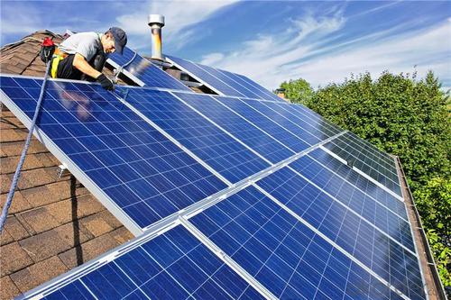
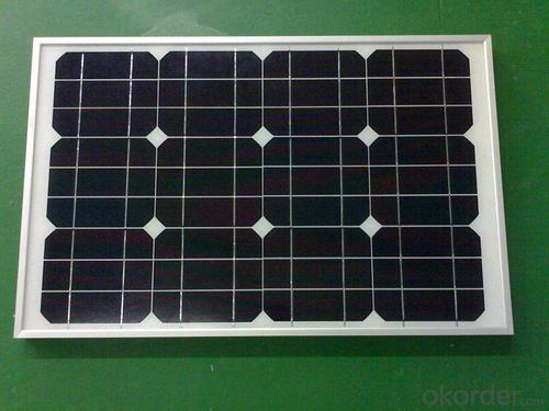

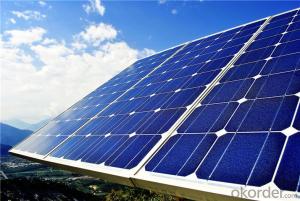
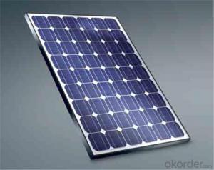
250W Solar Silicon Wafer Panels for Home Use Solar Power System
- Ref Price:
-

- Loading Port:
- China main port
- Payment Terms:
- TT OR LC
- Min Order Qty:
- 10000 watt
- Supply Capability:
- 20000000 watt/month
OKorder Service Pledge
OKorder Financial Service
You Might Also Like


Destription:
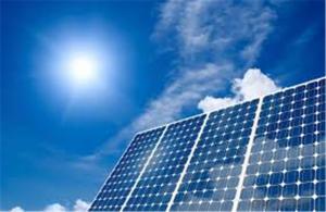
Solar panel refers to a panel designed to absorb the sun's rays as a source of energy for generating electricity or heating. A PV module is a packaged, connected assembly of typically 6×10 solar cells. Solar PV panels constitute the solar array of a photovoltaic system that generates and supplies solar electricity in commercial and residential applications.
Main Characteristic
1.Manufactured according to international quality and Environment Management
System (ISO9001, ISO14001)
2. By the high transmittance, low iron tempered glass, anti-aging of the EVA(polyethylene - vinyl acetate), high-performance crystalline silicon solar cells, good Weather resistance TPT (fluoroplastics composite membrane) by pyramid , has a good Weather resistance and anti-UV, hail, water-proof capacity.
3. OEM and customerized package are accepted
4. High efficiency crystalline silicon solar cells
Quality warranty
1.10 years limited warranty on material and workmanship
2. more than 90% power output in 10 years
3. more than 80% power output in 25 years
Product show


- Q: What is the role of back contact in solar silicon wafers?
- The role of back contact in solar silicon wafers is to provide electrical connection and support for the flow of current generated by the photovoltaic cells. It acts as a conductive layer that allows the captured solar energy to be efficiently transferred to external circuitry for use or storage. Additionally, it helps in maintaining the structural integrity of the wafer and protects the sensitive layers of the solar cell from external factors such as moisture and physical damage.
- Q: I would like to ask: silicon annealing treatment is how? Why anneal? Does annealing have an effect on the resistivity and the minority lifetime?
- Another fact: if the same "complement", can be understood as: oxygen from the surface after the removal of impurities, near the surface of the reduced defects is also reduced, the mean free path of carrier mobility increases, also increases, which leads to the decrease of resistivity.
- Q: What are the advantages of using a solar silicon wafer?
- One of the main advantages of using a solar silicon wafer is its high efficiency in converting sunlight into electricity. Silicon wafers have excellent electrical properties and can absorb a wide range of solar wavelengths, maximizing energy conversion. Additionally, silicon is abundant and readily available, making it a cost-effective option for solar panel manufacturing. Furthermore, silicon wafers are durable and have a long lifespan, ensuring reliable power generation for many years.
- Q: Are there any limitations to using solar silicon wafers in solar cells?
- Yes, there are several limitations to using solar silicon wafers in solar cells. One limitation is the high cost of producing silicon wafers, making solar cells more expensive compared to other energy sources. Additionally, silicon wafers are rigid and bulky, which limits their application in certain solar cell designs. Another limitation is the efficiency of silicon-based solar cells, as they have lower conversion efficiencies compared to emerging solar technologies like thin-film solar cells. Furthermore, the production of silicon wafers requires a significant amount of energy, contributing to the carbon footprint of solar cell manufacturing. Overall, while silicon wafers are widely used, their limitations highlight the need for ongoing research and development to enhance solar cell technologies.
- Q: How are solar silicon wafers protected from chemical damage?
- Solar silicon wafers are protected from chemical damage through the use of passivation layers and protective coatings. These layers act as a barrier, preventing chemical reactions from occurring between the silicon and external substances. Additionally, the wafers are often stored in controlled environments to minimize exposure to harmful chemicals and moisture.
- Q: Can solar silicon wafers be used in floating solar panel installations?
- Yes, solar silicon wafers can be used in floating solar panel installations. Floating solar panels typically use photovoltaic cells, which are made of silicon wafers. These wafers are specifically designed to convert sunlight into electricity, making them suitable for floating solar panel systems.
- Q: The purpose and means of chemical etching of silicon wafers?
- After slicing and grinding, the surface of silicon wafer has a layer of damage and pollution due to processing stress
- Q: Can solar silicon wafers be used in solar-powered water treatment plants?
- Yes, solar silicon wafers can be used in solar-powered water treatment plants. These wafers are commonly used in photovoltaic panels to convert sunlight into electricity. In a solar-powered water treatment plant, the solar silicon wafers can be utilized to generate the necessary energy to power the treatment processes, such as filtration, disinfection, and desalination.
- Q: What is the role of solar silicon wafers in reducing the digital divide?
- Solar silicon wafers play a crucial role in reducing the digital divide by facilitating the production of affordable and sustainable solar panels. These panels can be used to generate electricity in remote and underserved areas where access to the power grid is limited. By harnessing solar energy, these communities can power devices such as computers, smartphones, and other digital technologies, thus bridging the gap in access to information and communication. Solar silicon wafers enable the production of cost-effective solar panels, expanding the reach of clean and renewable energy solutions, and contributing to narrowing the digital divide.
- Q: How is an interconnect created in a solar silicon wafer?
- An interconnect in a solar silicon wafer is created by first depositing a thin layer of metal, such as silver or aluminum, onto the wafer's surface. This metal layer is then patterned and etched to form the desired interconnect structure, typically a grid-like pattern. The interconnect serves as a pathway for the flow of electrical current in the solar cell, allowing it to be efficiently connected to other cells and the overall solar panel system.
Send your message to us
250W Solar Silicon Wafer Panels for Home Use Solar Power System
- Ref Price:
-
- Loading Port:
- China main port
- Payment Terms:
- TT OR LC
- Min Order Qty:
- 10000 watt
- Supply Capability:
- 20000000 watt/month
OKorder Service Pledge
OKorder Financial Service
Similar products

Hot products


Hot Searches
Related keywords

