


Monocrystalline Silicon Wafer, Solar Wafer, 156*156mm
- Ref Price:
-

- Loading Port:
- China Main Port
- Payment Terms:
- TT or LC
- Min Order Qty:
- 100 Pcs PCS
- Supply Capability:
- 700 MW/Per Year PCS/month
OKorder Service Pledge
OKorder Financial Service
You Might Also Like


Specification of Mono Silicon Wafer
We can provide you solar wafer 156*156mm Mono Wafers for your raw materials choice.
| Product name | Mono Wafer |
| Conductive type | P type |
| Square size wafer(mm) | 156×156±0.5 |
| Resistivity | 1~3 ohm |
| Corner(mm) | 150±0.5;165±0.5 |
| 195±0.5;200±0.5 | |
| Thickness (μm) | 200±20 |
| Total thickness(um) | ≤ 30 |
| Resistivity range(Ωcm) | 1-3 |
| Doping elements | Boron |
| Orientation | (100)±1° |
| Carbon content(atoms/cc) | ≤1.0E+17 |
| Oxygen content(atoms/cc) | ≤1.0E+18 |
| Lifetime(μs) | ≥10 |
| Surface quality | No crack, gap, missing Angle, perforated, silicon fell and stress |
| Warping degrees(warp/μm) | ≤50 |
| Neighbouring vertical degree | 90±0.5° |
| Side damage(mm) | ≤0.5mm(length)×0.3mm(width)(not more than 2 per wafer) |
| Line mark(μm) | ≤15 |
Usage and Applications of Mono Wafers
Mono Solar Wafer mainly used in Mono Solar Cells with reliable quality and trustful efficiency performance. Our Mono Wafers should be your best choice for raw materials.
Packaging & Delivery of Mono Wafers
Carton Box Package and Deliver by air. Mono Wafers should be avoid of sunshine, moist, and water.
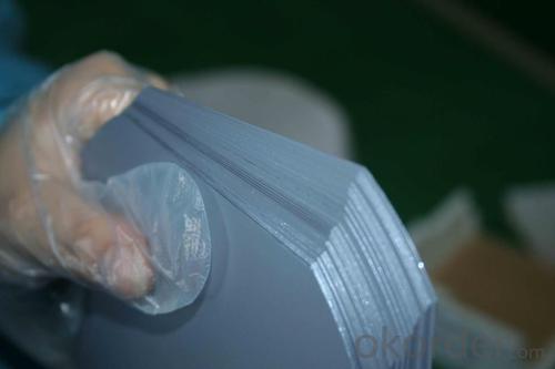
Factory Picture of Mono Wafers

Package Picture of Mono Wafers

- Q: Are there any initiatives to reduce the environmental impact of solar silicon wafer production?
- Yes, there are various initiatives aimed at reducing the environmental impact of solar silicon wafer production. These include the development and adoption of more sustainable manufacturing processes, such as the use of renewable energy sources in production facilities, reducing water usage, and implementing recycling programs for waste materials. Additionally, research is being conducted to explore alternative materials and techniques that could further minimize the environmental footprint of solar silicon wafer production.
- Q: Can solar silicon wafers be used in concentrated photovoltaics (CPV)?
- Yes, solar silicon wafers can be used in concentrated photovoltaics (CPV) systems. CPV systems use lenses or mirrors to concentrate sunlight onto solar cells, increasing their efficiency. While CPV typically relies on multi-junction solar cells, which are more efficient than traditional silicon-based solar cells, silicon wafers can still be used in CPV systems to generate electricity.
- Q: Are solar silicon wafers affected by power outages?
- No, solar silicon wafers are not directly affected by power outages since they do not rely on external power sources. They generate electricity from sunlight by converting photons into electrons, without the need for an active power supply. However, during a power outage, the solar panels themselves will not produce electricity unless they are connected to a functioning grid or have an energy storage system like batteries in place.
- Q: What is the silicon wafer, the specific definition of what?
- The chips made of silicon chips are amazingly powerful. The development of science and technology is driving the development of semiconductors. With the development of automation and computer technology, the cost of this kind of high technology product of silicon chip (integrated circuit) has been reduced to a very low level.
- Q: How are solar silicon wafers protected from electrical surges?
- Solar silicon wafers are protected from electrical surges through the use of protective devices such as surge arresters or varistors. These devices are connected in parallel with the solar cells and act as voltage clamps, diverting excess electrical energy away from the wafers. This helps prevent damage to the delicate silicon material and ensures the longevity and reliability of the solar panels.
- Q: How are solar silicon wafers affected by dust or dirt accumulation?
- Solar silicon wafers are negatively affected by dust or dirt accumulation as it reduces the amount of sunlight reaching the surface of the wafers, thereby reducing their efficiency in converting solar energy into electricity. Dust or dirt can create a barrier between the sunlight and the silicon material, resulting in decreased power output and overall performance of the solar cells. Hence, regular cleaning and maintenance are necessary to ensure optimal functioning of solar panels.
- Q: I would like to ask the solar cell (silicon) production process is the principle of how
- Solar cell production processThe production process of solar cell can be divided into three parts: silicon wafer testing, surface texturing, diffusion bonding, phosphorus removal, silica glass, plasma etching, antireflection coating, screen printing, rapid sintering and so on. Details are as follows:
- Q: What is the expected efficiency improvement for tandem quantum dot-silicon solar silicon wafers?
- The expected efficiency improvement for tandem quantum dot-silicon solar silicon wafers is significant. These wafers utilize quantum dots to enhance the absorption of sunlight, allowing for higher efficiency in converting solar energy into electricity. With the combination of quantum dot and silicon technologies, it is anticipated that the overall efficiency of these tandem wafers will be substantially higher compared to traditional silicon solar cells.
- Q: What is the role of emitter diffusion in solar silicon wafers?
- The role of emitter diffusion in solar silicon wafers is to create a region with a high concentration of dopant atoms, typically phosphorous or boron, in order to establish a pn junction. This junction is crucial for the conversion of sunlight into electricity, as it enables the separation and movement of charge carriers, resulting in the generation of a photovoltaic current.
- Q: What's the difference between a silicon wafer and a battery?
- Silicon chip, is a large piece of silicon, cut into a filmSolar cell, the mainstream is the silicon wafer made of crystalline silicon solar cells, or other solar cells: thin film solar cells, amorphous silicon solar energy, solar cells and so on
1. Manufacturer Overview
| Location | |
| Year Established | |
| Annual Output Value | |
| Main Markets | |
| Company Certifications |
2. Manufacturer Certificates
| a) Certification Name | |
| Range | |
| Reference | |
| Validity Period |
3. Manufacturer Capability
| a) Trade Capacity | |
| Nearest Port | |
| Export Percentage | |
| No.of Employees in Trade Department | |
| Language Spoken: | |
| b) Factory Information | |
| Factory Size: | |
| No. of Production Lines | |
| Contract Manufacturing | |
| Product Price Range | |
Send your message to us
Monocrystalline Silicon Wafer, Solar Wafer, 156*156mm
- Ref Price:
-
- Loading Port:
- China Main Port
- Payment Terms:
- TT or LC
- Min Order Qty:
- 100 Pcs PCS
- Supply Capability:
- 700 MW/Per Year PCS/month
OKorder Service Pledge
OKorder Financial Service
Similar products


Hot products


Hot Searches

