


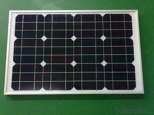
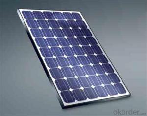
260W Silicon Wafer Based Solar Panels for Home Use Solar Power System
- Ref Price:
-

- Loading Port:
- China main port
- Payment Terms:
- TT OR LC
- Min Order Qty:
- 10000 watt
- Supply Capability:
- 20000000 watt/month
OKorder Service Pledge
OKorder Financial Service
You Might Also Like


Destription:
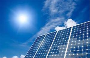
Solar panel refers to a panel designed to absorb the sun's rays as a source of energy for generating electricity or heating. A PV module is a packaged, connected assembly of typically 6×10 solar cells. Solar PV panels constitute the solar array of a photovoltaic system that generates and supplies solar electricity in commercial and residential applications.
Main Characteristic
1.Manufactured according to international quality and Environment Management
System (ISO9001, ISO14001)
2. By the high transmittance, low iron tempered glass, anti-aging of the EVA(polyethylene - vinyl acetate), high-performance crystalline silicon solar cells, good Weather resistance TPT (fluoroplastics composite membrane) by pyramid , has a good Weather resistance and anti-UV, hail, water-proof capacity.
3. OEM and customerized package are accepted
4. High efficiency crystalline silicon solar cells
Quality warranty
1.10 years limited warranty on material and workmanship
2. more than 90% power output in 10 years
3. more than 80% power output in 25 years
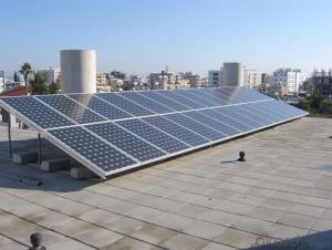
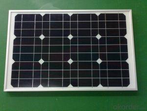
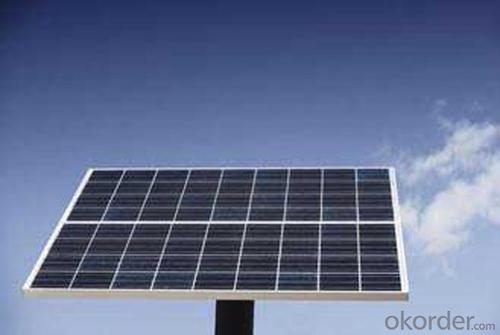
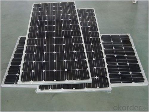
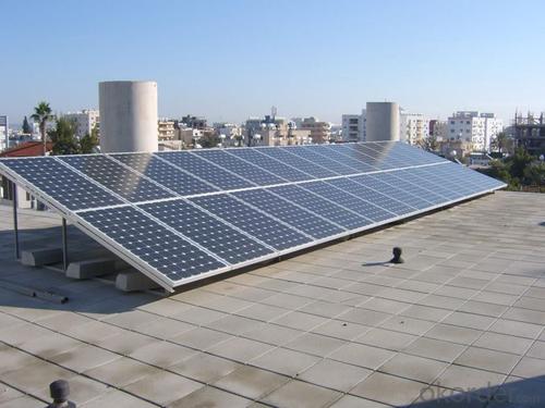
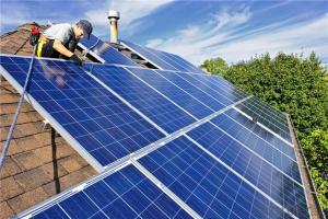
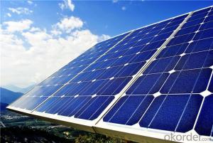
Product show


- Q: How do solar silicon wafers perform in sandy environments?
- Solar silicon wafers perform well in sandy environments as they are designed to be highly durable and resistant to various environmental conditions. The solid construction and protective coatings of the wafers help minimize the negative effects of sand particles, such as scratching or obstructing the surface. However, it is still important to regularly clean the panels to maintain optimal performance and ensure that sand accumulation does not significantly reduce their efficiency.
- Q: How are solar silicon wafers protected from moisture during storage?
- Solar silicon wafers are typically protected from moisture during storage by encapsulating them in a protective packaging such as airtight bags or containers with desiccants. This helps to prevent any moisture from coming into contact with the wafers, which could potentially degrade their performance or cause damage.
- Q: Can solar silicon wafers be used in portable solar panels?
- Yes, solar silicon wafers can be used in portable solar panels.
- Q: How are solar silicon wafers affected by temperature-induced stress?
- Solar silicon wafers are affected by temperature-induced stress in several ways. Firstly, as the temperature increases, the silicon wafer expands, leading to thermal expansion stress. This stress can cause cracking or warping of the wafer, affecting its structural integrity. Secondly, temperature fluctuations can also result in differential expansion between the silicon and other materials in the solar cell, leading to stress at the interfaces. This can cause delamination or detachment of the layers, impairing the performance of the solar cell. Finally, extreme temperature variations can induce thermal fatigue, gradually weakening the wafer over time and reducing its overall lifespan. Therefore, careful consideration and mitigation of temperature-induced stress are crucial in ensuring the reliability and efficiency of solar silicon wafers.
- Q: What are the different types of solar silicon wafers available?
- There are primarily three types of solar silicon wafers available: monocrystalline, polycrystalline, and thin-film. Monocrystalline wafers are made from a single crystal structure, offering high efficiency and a uniform appearance. Polycrystalline wafers are made from multiple crystal structures, providing slightly lower efficiency but at a lower cost. Thin-film wafers are made by depositing a thin layer of semiconductor material onto a substrate, offering flexibility and lower manufacturing costs, although with lower efficiency compared to crystalline wafers.
- Q: How are solar silicon wafers protected from extreme weather events?
- Solar silicon wafers are typically protected from extreme weather events through the use of encapsulants and protective coatings. These materials shield the wafers from moisture, UV radiation, and temperature fluctuations, ensuring their durability and longevity in various weather conditions. Additionally, solar panels are designed and installed with robust mounting systems to withstand strong winds, storms, and other extreme weather events.
- Q: What is the role of back surface field (BSF) in solar silicon wafers?
- The role of the back surface field (BSF) in solar silicon wafers is to enhance the efficiency of the solar cell by reducing the recombination of charge carriers. The BSF layer is typically formed by depositing a thin layer of dopants on the back surface of the silicon wafer. This layer acts as a barrier, preventing the recombination of the charge carriers (electrons and holes) generated by sunlight. By minimizing recombination, the BSF layer helps to increase the overall efficiency of the solar cell by ensuring that a higher proportion of the generated charge carriers can be collected and converted into electricity.
- Q: Can solar silicon wafers be used in other electronic devices?
- Yes, solar silicon wafers can be used in other electronic devices. These wafers are commonly used to manufacture solar cells for solar panels, but they can also be utilized in various other electronic applications such as integrated circuits, sensors, and microchips. The high purity and quality of solar silicon wafers make them suitable for use in a wide range of electronic devices.
- Q: What is the purpose of a temperature coefficient in a solar silicon wafer?
- The purpose of a temperature coefficient in a solar silicon wafer is to measure and understand how the wafer's performance and efficiency may be affected by changes in temperature. It allows manufacturers and users to determine the optimal operating conditions for the solar wafer in order to maximize its power output and overall performance.
- Q: Can solar silicon wafers be used in space exploration missions?
- Yes, solar silicon wafers can be used in space exploration missions.
Send your message to us
260W Silicon Wafer Based Solar Panels for Home Use Solar Power System
- Ref Price:
-
- Loading Port:
- China main port
- Payment Terms:
- TT OR LC
- Min Order Qty:
- 10000 watt
- Supply Capability:
- 20000000 watt/month
OKorder Service Pledge
OKorder Financial Service
Similar products

Hot products


Hot Searches
Related keywords

