
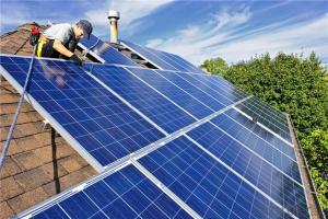


240w Solar Silicon Wafer Carrier Panel for Home Use Solar Power System
- Ref Price:
-

- Loading Port:
- China main port
- Payment Terms:
- TT OR LC
- Min Order Qty:
- 10000 watt
- Supply Capability:
- 20000000 watt/month
OKorder Service Pledge
OKorder Financial Service
You Might Also Like


Destription:
Solar panel refers to a panel designed to absorb the sun's rays as a source of energy for generating electricity or heating. A PV module is a packaged, connected assembly of typically 6×10 solar cells. Solar PV panels constitute the solar array of a photovoltaic system that generates and supplies solar electricity in commercial and residential applications.
Main Characteristic
1.Manufactured according to international quality and Environment Management
System (ISO9001, ISO14001)
2. By the high transmittance, low iron tempered glass, anti-aging of the EVA(polyethylene - vinyl acetate), high-performance crystalline silicon solar cells, good Weather resistance TPT (fluoroplastics composite membrane) by pyramid , has a good Weather resistance and anti-UV, hail, water-proof capacity.
3. OEM and customerized package are accepted
4. High efficiency crystalline silicon solar cells
Quality warranty
1.10 years limited warranty on material and workmanship
2. more than 90% power output in 10 years
3. more than 80% power output in 25 years
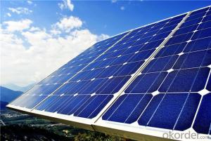
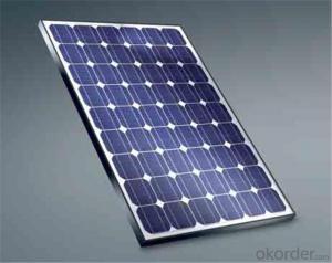
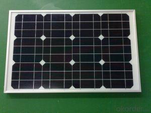
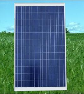
Product show


- Q: Are there any initiatives to reduce the environmental impact of solar silicon wafer production?
- Yes, there are various initiatives aimed at reducing the environmental impact of solar silicon wafer production. These include the development and adoption of more sustainable manufacturing processes, such as the use of renewable energy sources in production facilities, reducing water usage, and implementing recycling programs for waste materials. Additionally, research is being conducted to explore alternative materials and techniques that could further minimize the environmental footprint of solar silicon wafer production.
- Q: Can solar silicon wafers be used in solar-powered space vehicles?
- Yes, solar silicon wafers can be used in solar-powered space vehicles. Solar silicon wafers are commonly used in photovoltaic systems to convert sunlight into electricity. In space, where there is abundant sunlight, solar panels made with silicon wafers can efficiently capture and convert solar energy into electrical power to operate various systems and equipment onboard the space vehicles.
- Q: How is a front contact applied to a solar silicon wafer?
- A front contact is typically applied to a solar silicon wafer through a process known as screen printing. In this method, a special paste containing conductive materials such as silver or aluminum is spread onto the surface of the wafer using a mesh screen. The screen is carefully aligned with the wafer, and the paste is forced through the screen onto the wafer surface using a squeegee or a similar tool. This creates a pattern of conductive lines that make up the front contact. The paste is then dried and cured, forming a solid and durable front contact layer on the solar wafer.
- Q: How to calculate the conversion efficiency of monocrystalline silicon
- Solar cell efficiency = (open circuit voltage * short-circuit voltage * fill factor) / (battery area * light amplitude) *100%Light intensity - AM1.5 as the standard, that is 1000W/m2Proportion of dark current - Irev>6 cell ratioThe proportion of low efficiency tablets - the proportion of P156Eff<14.5% batteries
- Q: What is the role of a solar silicon wafer in a solar cell?
- The role of a solar silicon wafer in a solar cell is to serve as the substrate or base material where the photovoltaic process takes place. The silicon wafer is typically doped with impurities to create a p-n junction, which allows for the conversion of sunlight into electricity. It acts as the main absorber of light, generating electron-hole pairs when photons hit its surface. These electron-hole pairs are then separated and directed by the electric field within the solar cell, ultimately producing an electric current.
- Q: What is the role of back surface field (BSF) in solar silicon wafers?
- The role of back surface field (BSF) in solar silicon wafers is to enhance the efficiency of the solar cell by reducing recombination losses at the rear surface of the wafer. It creates a high-quality passivation layer that helps to minimize carrier recombination and improves the collection of photogenerated charge carriers, resulting in improved overall solar cell performance.
- Q: What is the role of light trapping in solar silicon wafers?
- The role of light trapping in solar silicon wafers is to increase the absorption of sunlight and enhance the efficiency of the solar cells. Light trapping techniques, such as texturing or adding anti-reflective coatings, help to reduce the reflection and scattering of light, allowing more photons to be absorbed by the silicon material. This allows the solar cells to convert a higher percentage of the incident light into usable electrical energy.
- Q: Can solar silicon wafers be used in agricultural irrigation systems?
- Yes, solar silicon wafers can be used in agricultural irrigation systems. They can be utilized to power solar panels that generate electricity, which can then be used to run pumps and other equipment needed for irrigation.
- Q: What is the role of a glass cover in a solar silicon wafer?
- The role of a glass cover in a solar silicon wafer is to protect the wafer from external environmental factors such as dust, moisture, and mechanical damage. It provides a barrier that prevents the silicon wafer from getting scratched, contaminated, or oxidized, which could negatively impact its performance and efficiency. Additionally, the glass cover helps to optimize the transmission of sunlight onto the silicon wafer, enhancing the absorption of solar energy and maximizing the overall power output of the solar cell.
- Q: What is the typical thickness tolerance of a solar silicon wafer?
- The typical thickness tolerance of a solar silicon wafer is around 20-30 micrometers.
Send your message to us
240w Solar Silicon Wafer Carrier Panel for Home Use Solar Power System
- Ref Price:
-
- Loading Port:
- China main port
- Payment Terms:
- TT OR LC
- Min Order Qty:
- 10000 watt
- Supply Capability:
- 20000000 watt/month
OKorder Service Pledge
OKorder Financial Service
Similar products

Hot products


Hot Searches
Related keywords

