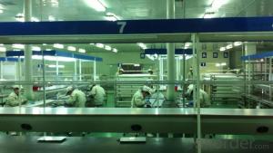
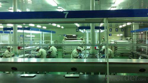


Ic Grade Solar Silicon Wafer Supplier - High Quality A Grade Mono Crystalline 5V 17.8% Solar Cell
- Ref Price:
-

- Loading Port:
- Shanghai
- Payment Terms:
- TT OR LC
- Min Order Qty:
- 1000 pc
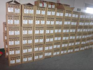
- Supply Capability:
- 100000 pc/month
OKorder Service Pledge
OKorder Financial Service
You Might Also Like


Specifications
hot sale solar cell
1.16.8%~18.25% high efficiency
2.100% checked quality
3.ISO9001/ISO14001/TUV/CE/UL
4.stable performance
We can offer you the best quality products and services, don't miss !
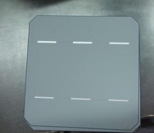
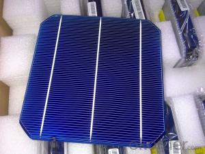
POLY6'(156*156)
Polycrystalline Silicon Solar cell
Physical Characteristics
Dimension: 156mm×156mm±0.5mm
Diagonal: 220mm±0.5mm
Thickness(Si): 200±20 μm
Front(-) Back(+)
Blue anti-reflecting coating (silicon nitride); Aluminum back surface field;
1.5mm wide bus bars; 2.0mm wide soldering pads;
Distance between bus bars: 51mm . Distance between bus bars :51mm .
Electrical Characteristics
Efficiency(%) | 18.00 | 17.80 | 17.60 | 17.40 | 17.20 | 16.80 | 16.60 | 16.40 | 16.20 | 16.00 | 15.80 | 15.60 |
Pmpp(W) | 4.33 | 4.29 | 4.24 | 4.19 | 4.14 | 4.09 | 4.04 | 3.99 | 3.94 | 3.90 | 3.86 | 3.82 |
Umpp(V) | 0.530 | 0.527 | 0.524 | 0.521 | 0.518 | 0.516 | 0.514 | 0.511 | 0.509 | 0.506 | 0.503 | 0.501 |
Impp(A) | 8.159 | 8.126 | 8.081 | 8.035 | 7.990 | 7.938 | 7.876 | 7.813 | 7.754 | 7.698 | 7.642 | 7.586 |
Uoc(V) | 0.633 | 0.631 | 0.628 | 0.625 | 0.623 | 0.620 | 0.618 | 0.617 | 0.615 | 0.613 | 0.611 | 0.609 |
Isc(A) | 8.709 | 8.677 | 8.629 | 8.578 | 8.531 | 8.478 | 8.419 | 8.356 | 8.289 | 8.220 | 8.151 | 8.083 |

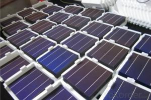
MONO5'(125*125mm)165
Monocrystalline silicon solar cell
Physical Characteristics
Dimension: 125mm×125mm±0.5mm
Diagonal: 165mm±0.5mm
Thickness(Si): 200±20 μm
Front(-) Back(+)
Blue anti-reflecting coating(silicon nitride); Aluminum back surface field;
1.6mmwide bus bars; 2.5mm wide soldering pads;
Distance between bus bars: 61mm . Distance between bus bars :61mm .
Electrical Characteristics
Efficiency(%) | 19.40 | 19.20 | 19.00 | 18.80 | 18.60 | 18.40 | 18.20 | 18.00 | 17.80 | 17.60 | 17.40 | 17.20 |
Pmpp(W) | 2.97 | 2.94 | 2.91 | 2.88 | 2.85 | 2.82 | 2.79 | 2.76 | 2.73 | 2.70 | 2.67 | 2.62 |
Umpp(V) | 0.537 | 0.535 | 0.533 | 0.531 | 0.527 | 0.524 | 0.521 | 0.518 | 0.516 | 0.515 | 0.513 | 0.509 |
Impp(A) | 5.531 | 5.495 | 5.460 | 5.424 | 5.408 | 5.382 | 5.355 | 5.328 | 5.291 | 5.243 | 5.195 | 4.147 |
Uoc(V) | 0.637 | 0.637 | 0.636 | 0.635 | 0.633 | 0.630 | 0.629 | 0.629 | 0.628 | 0.626 | 0.626 | 0.625 |
Isc(A) | 5.888 | 5.876 | 5.862 | 5.848 | 5.839 | 5.826 | 5.809 | 5.791 | 5.779 | 5.756 | 5.293 | 5.144 |

FAQ:
Q:How can i get some sample?
A:Yes , if you want order ,sample is not a problem.
Q:How about your solar panel efficency?
A: Our product efficency around 17.25%~18.25%.
Q:What’s the certificate you have got?
A: we have overall product certificate of ISO9001/ISO14001/CE/TUV/UL
- Q: Can solar silicon wafers be used in concentrated solar power systems?
- Yes, solar silicon wafers can be used in concentrated solar power systems. These wafers are typically used in photovoltaic systems to generate electricity directly from sunlight. In concentrated solar power systems, the sunlight is focused onto a small area to produce heat, which can then be used to generate electricity through various methods such as steam turbines. While solar silicon wafers may not be the primary component in concentrated solar power systems, they can still play a role in certain aspects of the system, such as in the conversion of the concentrated solar energy into electricity.
- Q: How are solar silicon wafers handled and transported?
- Solar silicon wafers are typically handled and transported with great care to protect their fragile nature. They are usually packaged in protective cases or trays to prevent damage during handling and transportation. Specialized equipment, such as robotic arms or vacuum grippers, may be used to move and manipulate the wafers without causing any harm. Additionally, they are often transported in climate-controlled environments to prevent exposure to extreme temperatures or humidity, which can affect their performance.
- Q: How do solar silicon wafers perform in extreme weather conditions?
- Solar silicon wafers generally perform well in extreme weather conditions. They are designed to withstand high temperatures, humidity, and even harsh weather elements such as snow and hail. However, extreme conditions like excessive heat or cold can slightly affect their efficiency. Overall, solar silicon wafers are engineered to be durable and reliable, making them suitable for various weather conditions.
- Q: What is the impact of crystal orientation on solar silicon wafers?
- The impact of crystal orientation on solar silicon wafers is significant. The orientation of the crystal lattice in the wafer determines its electrical properties and overall efficiency as a solar cell. Different crystal orientations can affect the recombination rate, carrier mobility, and light absorption capabilities of the wafer. For instance, certain orientations like (100) or (111) exhibit higher light absorption, while others may have better charge carrier transport properties. Therefore, optimizing the crystal orientation during the manufacturing process is crucial to enhance the performance and yield of solar silicon wafers.
- Q: What is the effect of spectral response on the efficiency of a solar silicon wafer?
- The spectral response of a solar silicon wafer refers to its ability to convert different wavelengths of light into electricity. The efficiency of a solar silicon wafer is directly influenced by its spectral response. If the wafer has a broad and high spectral response, it can capture a wider range of solar radiation and convert it into electricity more efficiently. However, if the spectral response is limited or low, the wafer may not be able to effectively utilize certain wavelengths of light, resulting in lower overall efficiency. Therefore, a higher spectral response generally leads to a more efficient solar silicon wafer.
- Q: Can solar silicon wafers be used in floating solar panel installations?
- Yes, solar silicon wafers can be used in floating solar panel installations. These wafers are commonly used in traditional solar panel systems and can also be adapted for floating installations. The key difference lies in the mounting structure and anchoring mechanisms, which are designed to keep the panels afloat on bodies of water.
- Q: What is the role of solar silicon wafers in disaster response and recovery?
- Solar silicon wafers play a crucial role in disaster response and recovery by providing a reliable source of clean energy. These wafers are used to manufacture solar panels, which can be quickly deployed in disaster-stricken areas to generate electricity. This renewable energy source helps power emergency response efforts, including communication systems, lighting, medical equipment, and water purification systems. Solar silicon wafers enable more sustainable and resilient disaster response, reducing dependence on traditional power sources and ensuring a continuous supply of electricity in times of crisis.
- Q: Are there any initiatives to improve the sustainability of solar silicon wafers?
- Yes, there are several initiatives aimed at improving the sustainability of solar silicon wafers. These initiatives focus on various aspects such as reducing the energy consumption and environmental impact of the manufacturing process, increasing the efficiency and lifespan of the wafers, and developing recycling technologies to minimize waste. Additionally, research and development efforts are underway to explore alternative materials and manufacturing techniques that could further enhance the sustainability of solar silicon wafers.
- Q: How to do on the silicon wafer
- The general use of ultrasonic and pre cleaning (pickling) can be solved
- Q: What is the typical lead time for ordering solar silicon wafers?
- The typical lead time for ordering solar silicon wafers can vary depending on various factors such as supplier availability, quantity ordered, and any custom requirements. However, on average, it can range from a few weeks to a few months.
Send your message to us
Ic Grade Solar Silicon Wafer Supplier - High Quality A Grade Mono Crystalline 5V 17.8% Solar Cell
- Ref Price:
-
- Loading Port:
- Shanghai
- Payment Terms:
- TT OR LC
- Min Order Qty:
- 1000 pc
- Supply Capability:
- 100000 pc/month
OKorder Service Pledge
OKorder Financial Service
Similar products


Hot products


Hot Searches
Related keywords

