


Monocrystalline Solar Silicon Wafer - High Quality A Grade Cell Polyrystalline 5V 17.6%
- Ref Price:
-

- Loading Port:
- Shanghai
- Payment Terms:
- TT OR LC
- Min Order Qty:
- 1000 pc
- Supply Capability:
- 100000 pc/month
OKorder Service Pledge
OKorder Financial Service
You Might Also Like


Specifications
hot sale solar cell
1.16.8%~18.25% high efficiency
2.100% checked quality
3.ISO9001/ISO14001/TUV/CE/UL
4.stable performance
We can offer you the best quality products and services, don't miss !
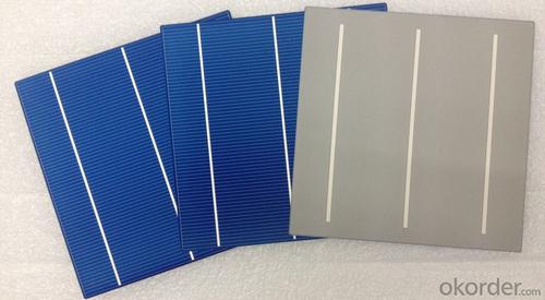
POLY6'(156*156)
Polycrystalline Silicon Solar cell
Physical Characteristics
Dimension: 156mm×156mm±0.5mm
Diagonal: 220mm±0.5mm
Thickness(Si): 200±20 μm
Front(-) Back(+)
Blue anti-reflecting coating (silicon nitride); Aluminum back surface field;
1.5mm wide bus bars; 2.0mm wide soldering pads;
Distance between bus bars: 51mm . Distance between bus bars :51mm .
Electrical Characteristics
Efficiency(%) | 18.00 | 17.80 | 17.60 | 17.40 | 17.20 | 16.80 | 16.60 | 16.40 | 16.20 | 16.00 | 15.80 | 15.60 |
Pmpp(W) | 4.33 | 4.29 | 4.24 | 4.19 | 4.14 | 4.09 | 4.04 | 3.99 | 3.94 | 3.90 | 3.86 | 3.82 |
Umpp(V) | 0.530 | 0.527 | 0.524 | 0.521 | 0.518 | 0.516 | 0.514 | 0.511 | 0.509 | 0.506 | 0.503 | 0.501 |
Impp(A) | 8.159 | 8.126 | 8.081 | 8.035 | 7.990 | 7.938 | 7.876 | 7.813 | 7.754 | 7.698 | 7.642 | 7.586 |
Uoc(V) | 0.633 | 0.631 | 0.628 | 0.625 | 0.623 | 0.620 | 0.618 | 0.617 | 0.615 | 0.613 | 0.611 | 0.609 |
Isc(A) | 8.709 | 8.677 | 8.629 | 8.578 | 8.531 | 8.478 | 8.419 | 8.356 | 8.289 | 8.220 | 8.151 | 8.083 |

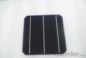
MONO5'(125*125mm)165
Monocrystalline silicon solar cell
Physical Characteristics
Dimension: 125mm×125mm±0.5mm
Diagonal: 165mm±0.5mm
Thickness(Si): 200±20 μm
Front(-) Back(+)
Blue anti-reflecting coating(silicon nitride); Aluminum back surface field;
1.6mmwide bus bars; 2.5mm wide soldering pads;
Distance between bus bars: 61mm . Distance between bus bars :61mm .
Electrical Characteristics
Efficiency(%) | 19.40 | 19.20 | 19.00 | 18.80 | 18.60 | 18.40 | 18.20 | 18.00 | 17.80 | 17.60 | 17.40 | 17.20 |
Pmpp(W) | 2.97 | 2.94 | 2.91 | 2.88 | 2.85 | 2.82 | 2.79 | 2.76 | 2.73 | 2.70 | 2.67 | 2.62 |
Umpp(V) | 0.537 | 0.535 | 0.533 | 0.531 | 0.527 | 0.524 | 0.521 | 0.518 | 0.516 | 0.515 | 0.513 | 0.509 |
Impp(A) | 5.531 | 5.495 | 5.460 | 5.424 | 5.408 | 5.382 | 5.355 | 5.328 | 5.291 | 5.243 | 5.195 | 4.147 |
Uoc(V) | 0.637 | 0.637 | 0.636 | 0.635 | 0.633 | 0.630 | 0.629 | 0.629 | 0.628 | 0.626 | 0.626 | 0.625 |
Isc(A) | 5.888 | 5.876 | 5.862 | 5.848 | 5.839 | 5.826 | 5.809 | 5.791 | 5.779 | 5.756 | 5.293 | 5.144 |

FAQ:
Q:How can i get some sample?
A:Yes , if you want order ,sample is not a problem.
Q:How about your solar panel efficency?
A: Our product efficency around 17.25%~18.25%.
Q:What’s the certificate you have got?
A: we have overall product certificate of ISO9001/ISO14001/CE/TUV/UL
- Q: How are solar silicon wafers protected from bird droppings?
- Solar silicon wafers are typically protected from bird droppings through the use of anti-reflective coatings, which make the surface less attractive for birds to perch on. Additionally, some solar installations may utilize bird deterrents such as netting or spikes to prevent birds from landing and potentially causing damage or soiling the wafers.
- Q: How do solar silicon wafers contribute to reducing the risk of power outages?
- Solar silicon wafers, which are the key component in solar panels, contribute to reducing the risk of power outages by harnessing solar energy and converting it into electricity. This renewable energy source helps diversify the power generation mix, reducing reliance on fossil fuels and decreasing the strain on the power grid. As solar panels generate electricity during the daytime, when demand is typically high, they help meet peak load requirements and prevent overloading or blackouts. By providing a decentralized and distributed energy source, solar silicon wafers enhance the resilience and reliability of the power system, mitigating the risk of power outages.
- Q: Are there any environmental concerns with the production or disposal of solar silicon wafers?
- Yes, there are some environmental concerns associated with the production and disposal of solar silicon wafers. The production of silicon wafers involves energy-intensive processes and the use of hazardous chemicals, which can contribute to air and water pollution if not managed properly. Additionally, the mining of raw materials for silicon wafers can have negative impacts on ecosystems and communities. Proper disposal and recycling of silicon wafers are also important to prevent potential environmental harm. However, it is worth noting that compared to other energy sources, the environmental impact of solar silicon wafers is relatively lower, and advancements in technology and regulations continue to address these concerns.
- Q: What is the impact of impurities on the reliability of solar silicon wafers?
- The presence of impurities in solar silicon wafers can significantly impact their reliability. Impurities can affect the electrical properties of the wafer, leading to decreased efficiency and performance of the solar cells. They can cause non-uniformity in the material, resulting in variations in cell performance within a module or across different modules. Moreover, impurities can also induce defects and degradation mechanisms that can reduce the lifespan of the solar cells. Therefore, minimizing impurities during the manufacturing process is crucial for ensuring the long-term reliability and efficiency of solar silicon wafers.
- Q: Can solar silicon wafers be used in building-integrated photovoltaics (BIPV)?
- Yes, solar silicon wafers can be used in building-integrated photovoltaics (BIPV). BIPV refers to the integration of solar panels or cells into the building envelope, such as windows, roofs, or facades. Silicon wafers are commonly used in the production of solar cells, including those used in BIPV systems. These wafers are processed to create solar cells, which can then be integrated into various building materials, allowing for the generation of solar power while also serving as functional building elements.
- Q: How much does a solar silicon wafer weigh?
- A solar silicon wafer typically weighs around 4 to 6 grams. However, the weight can vary depending on the size and thickness of the wafer.
- Q: Can solar silicon wafers be used in solar-powered wearable devices?
- Yes, solar silicon wafers can be used in solar-powered wearable devices. These wafers are commonly used to produce solar cells, which can be integrated into wearable devices to harness solar energy and power them. This allows for a sustainable and renewable energy source for these devices.
- Q: What is the difference between the purpose of wafer cleaning and the cleaning of silicon material, what is the difference between the acid used
- The silicon wafer cleaning is also known as the production of wool, chemical etching of silicon wafer surface, so that the light area
- Q: From raw materials to finished products processing and production of the main links? Construction technology? Key issues of safety in production? What security measures are generally taken?
- (4): end shoulder growth after a long thin neck, to reduce the temperature and casting speed, the crystal diameter gradually increased to the desired size. (5) the diameter growth: after a long neck and shoulder end, by continuously adjusting casting speed and temperature, the crystal diameter maintained at between 2mm positive and negative, the diameter of fixed part is called the diameter part. Monocrystalline silicon wafer from the equal diameter part. (6) tail growth: if the rod is separated from the liquid surface, the effect force will cause the dislocation and slip line of the crystal rod. So in order to avoid the occurrence of this problem, the diameter of the crystal rod must be gradually reduced until it is a sharp point and separated from the liquid surface. This process is called tail growth. After a long period of time, the crystal rod is taken out of the furnace chamber for cooling for a period of time to complete a growth cycle.
- Q: How are solar silicon wafers handled during installation?
- Solar silicon wafers are handled with utmost care during installation to ensure their integrity and efficiency. They are typically transported in protective packaging and handled with clean gloves to prevent any contamination. During installation, the wafers are carefully placed onto a mounting structure or integrated into solar panels, ensuring proper alignment and secure attachment. Attention is given to avoiding any scratches, cracks, or damage to the wafers, as these can significantly impact their performance and lifespan.
Send your message to us
Monocrystalline Solar Silicon Wafer - High Quality A Grade Cell Polyrystalline 5V 17.6%
- Ref Price:
-
- Loading Port:
- Shanghai
- Payment Terms:
- TT OR LC
- Min Order Qty:
- 1000 pc
- Supply Capability:
- 100000 pc/month
OKorder Service Pledge
OKorder Financial Service
Similar products


Hot products


Hot Searches
Related keywords

