


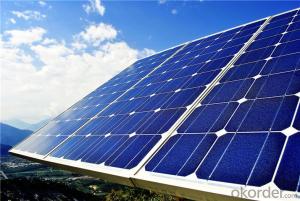
Silicon Wafer Solar Cell Panels - Monosolicion Poly 156mm*156mm
- Ref Price:
-

- Loading Port:
- China main port
- Payment Terms:
- TT OR LC
- Min Order Qty:
- 100 watt
- Supply Capability:
- 10000 watt/month
OKorder Service Pledge
Quality Product, Order Online Tracking, Timely Delivery
OKorder Financial Service
Credit Rating, Credit Services, Credit Purchasing
You Might Also Like


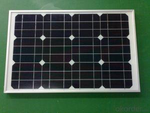
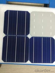
Monosolicion Solar Cells Poly 156mm*156mm
Typical electrical characteristics
Efficiency code | 1720 | 1740 | 1760 | 1780 | 1820 | 1840 | |
Efficiency (min) | (%) | 17.2 | 17.4 | 17.6 | 17.8 | 18.2 | 18.4 |
Pmax | (W) | 4.186 | 4.234 | 4.283 | 4.332 | 4.429 | 4.478 |
Voc | (V) | 0.631 | 0.632 | 0.634 | 0.636 | 0.640 | 0.642 |
Isc | (A) | 8.446 | 8.485 | 8.523 | 8.573 | 8.660 | 8.700 |
Vmp | (V) | 0.525 | 0.527 | 0.529 | 0.531 | 0.535 | 0.537 |
Imp | (A) | 7.973 | 8.035 | 8.097 | 8.160 | 8.280 | 8.340 |
Data under standard testing conditions(STC): 1,000W/m2, AM1.5, 25℃, Pmax: Positive power tolerance.
Typical teperature coefficients
Voltage | -2.08 | mV/K |
Current | +4.58 | mA/K |
Power | -0.40 | %/K |
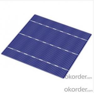
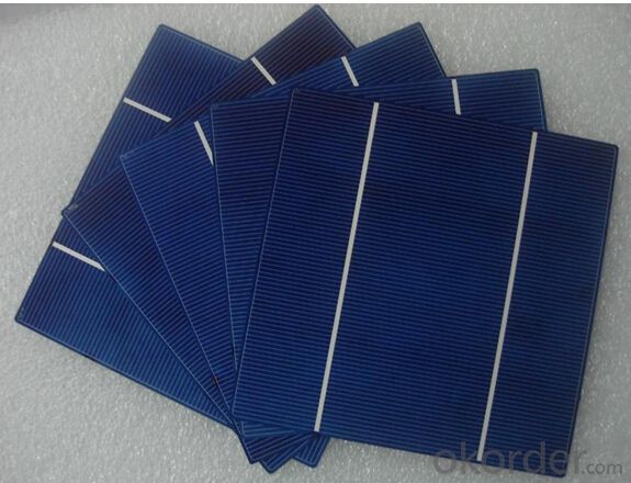
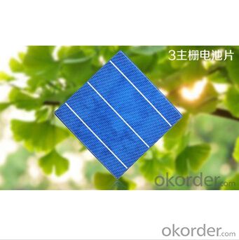
Cell Picture


- Q: Monocrystalline silicon processing technology
- Most photovoltaic equipment suppliers buy chip wire. They generally grow silicon ingots or silicon blocks and process silicon materials into wafers, which are eventually sold to photovoltaic cell manufacturers for the production of batteries. The installed capacity of the industry's most successful application of B5 wire materials company HCT system more than 500 units, is a benchmark in the field of photovoltaic chip products nclusionIn the field of photovoltaic technology, wire reduces wafer thickness and reduce the material loss in the cutting process, thereby reducing the power consumption of the solar silicon materials. (therefore, wire saw technology to reduce the cost per watt of solar energy and eventually to achieve grid parity has played a crucial role. The latest and most advanced wire technology brings a lot of innovation, improve the productivity and the thinner silicon wafers to reduce the consumption of silicon materials.
- Q: How are solar silicon wafers affected by temperature coefficient?
- Solar silicon wafers are affected by temperature coefficient in terms of their electrical properties. The temperature coefficient measures how the performance of the solar cell changes with temperature. A positive temperature coefficient means that as the temperature increases, the solar cell's efficiency decreases, resulting in a decrease in power output. Conversely, a negative temperature coefficient implies that as the temperature rises, the solar cell's efficiency increases, leading to an increase in power output. Therefore, the temperature coefficient plays a crucial role in determining the overall performance and power generation capabilities of solar silicon wafers.
- Q: How do solar silicon wafers handle extreme weather conditions like hailstorms?
- Solar silicon wafers are designed to withstand extreme weather conditions, including hailstorms. They are manufactured with a protective layer, typically made of tempered glass, which is highly durable and able to resist impacts from hailstones. Additionally, solar panels undergo rigorous testing to ensure they can handle various weather elements, including hailstorms, high winds, and temperature fluctuations. While hailstorms may cause superficial damage to the protective glass layer, the underlying silicon cells are often well-protected, and the overall performance of the solar panel is not significantly affected.
- Q: Pure curiosity why silicon wafer is round
- Why does the silicon grown in the melt not directly cut into square, it is not easy to put it......Rub... In order to reduce costs ah.
- Q: How do solar silicon wafers perform in high-temperature environments?
- Solar silicon wafers generally perform well in high-temperature environments. The crystalline structure of silicon allows it to handle high temperatures without significant loss in performance. However, excessive heat can cause a slight decrease in efficiency, and prolonged exposure to extreme temperatures can result in some degradation over time. To mitigate these effects, solar panels are often designed with cooling mechanisms and protective coatings to ensure reliable performance even in hot climates.
- Q: What is the expected efficiency improvement for multi-junction perovskite-silicon solar silicon wafers?
- The expected efficiency improvement for multi-junction perovskite-silicon solar silicon wafers is significant. These wafers have the potential to achieve much higher efficiencies compared to traditional silicon solar cells. With the combination of perovskite and silicon materials, the multi-junction design allows for better absorption of a wider range of wavelengths, leading to increased energy conversion. Although the exact improvement may vary depending on the specific design and manufacturing processes, it is anticipated that multi-junction perovskite-silicon solar silicon wafers could potentially achieve efficiencies beyond 30% or even higher.
- Q: What are the different types of solar silicon wafers available?
- There are mainly three types of solar silicon wafers available: monocrystalline, polycrystalline, and thin-film. Monocrystalline wafers are made from a single crystal structure, providing high efficiency but at a higher cost. Polycrystalline wafers are made from multiple crystal structures, offering slightly lower efficiency but at a more affordable price. Thin-film wafers are made by depositing a thin layer of semiconductor material onto a substrate, providing flexibility and lower manufacturing costs, but with lower efficiency compared to crystalline wafers.
- Q: How does the thickness of a front contact affect the efficiency of a solar silicon wafer?
- The thickness of a front contact on a solar silicon wafer directly affects the efficiency of the wafer. A thicker front contact can reduce the efficiency of a solar cell because it can increase the amount of light that is reflected off the surface of the wafer, preventing it from being absorbed and converted into electricity. On the other hand, a thinner front contact can improve efficiency by allowing more light to be absorbed and utilized by the solar cell. Therefore, finding the optimal thickness for the front contact is crucial in maximizing the efficiency of a solar silicon wafer.
- Q: How are solar silicon wafers protected from fire hazards?
- Solar silicon wafers are protected from fire hazards through the implementation of safety measures such as fire-resistant encapsulation materials, fire suppression systems, and proper installation techniques. These measures help prevent the ignition and spread of fires, ensuring the safety and reliability of solar panels.
- Q: What is a solar silicon wafer?
- A solar silicon wafer is a thin slice of crystalline silicon used as a substrate in the production of solar cells. It serves as the foundation for the deposition of various layers that make up the solar cell, allowing it to convert sunlight into electricity.
Send your message to us
Silicon Wafer Solar Cell Panels - Monosolicion Poly 156mm*156mm
- Ref Price:
-
- Loading Port:
- China main port
- Payment Terms:
- TT OR LC
- Min Order Qty:
- 100 watt
- Supply Capability:
- 10000 watt/month
OKorder Service Pledge
Quality Product, Order Online Tracking, Timely Delivery
OKorder Financial Service
Credit Rating, Credit Services, Credit Purchasing
Similar products


Hot products


Hot Searches
Related keywords

