
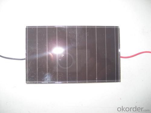
Thin Silicon Wafer Solar Cell - Amorphous Silicon Dice Specification 5
- Ref Price:
-

- Loading Port:
- China Main Port
- Payment Terms:
- TT OR LC
- Min Order Qty:
- -
- Supply Capability:
- -
OKorder Service Pledge
OKorder Financial Service
You Might Also Like


Pv modules at present, the mainstream products are still in silicon as the main raw materials, only in terms of silicon raw material consumption, production 1 mw of crystalline silicon solar cell, need 10 to 12 tons of high purity silicon, but if use the same silicon materials used to produce thin film amorphous silicon solar cell can produce more than 200 mw.
From the perspective of energy consumption, amorphous silicon solar battery only 1-1.5 years of energy recovery period, more embodies its contribution to energy saving in the manufacturing process.
Component occupies a high proportion of costs in a photovoltaic system, the component prices directly affect the system cost, and thus affect the cost of photovoltaic power generation. Calculated at the current price of components, the same money, buy amorphous silicon products, you can get more close to 30% of the power components.
2, more power
For the same power of solar cell array, amorphous silicon solar cell is about 10% more than monocrystalline silicon, polycrystalline silicon battery power. This has been the Uni - Solar System LLC, Energy Photovoltaic Corp., Japan's Kaneka Corp., the Netherlands Energy research institute, and other organizations and experts confirmed that the Photovoltaic industry.
In sunny, that is to say, under the high temperature, amorphous silicon solar cell components can show more excellent power performance.
3, better low light response
Due to the characteristics of amorphous silicon atoms are arranged disorderly, the electron transition no longer comply with the restriction of traditional \"selection rule\", as a result, its light absorption characteristics and there are big differences monocrystalline silicon material. Amorphous silicon and monocrystalline silicon material absorption curve as shown
, amorphous silicon absorption curve has obvious three sections (A, B, C). Area A corresponding electronic transition between localized states, such as the gap state near Fermi level and to the tail state transition, the absorption coefficient is small, about 1-10 cm - 1, for this is absorbing; B area absorption coefficient with the increase of the photon energy index rose, it corresponds to the electrons from the valence band edge extension state to the conduction band localized state transition, as well as the localized electrons from the valence band tail states guide for edge extension state transition, the region's energy range is usually only about half of the electron volts, but absorption coefficient across two or three orders of magnitude, usually up to 104 cm - 1; Area C corresponds to the electrons from the valence band to the conduction band internal internal transition, the absorption coefficient is bigger, often in more than 104 cm - 1. After two absorption area is crystalline silicon eigen absorption area.
Can be seen in the figure, the intersection of two curves about 1.8 ev. It is important to note that in the visible light range (1.7 to 3.0 ev), the absorption coefficient of amorphous silicon material is almost an order of magnitude larger than the single crystal silicon. That is to say, in the morning the first part of the sun is not too strong, the second half, and it's cloudy in the afternoon under the condition of low light intensity, long wave is greater, the amorphous silicon material still has a large absorption coefficient. Again considering the amorphous silicon band gap is larger, the reverse saturation current I0 is smaller. And as mentioned the amorphous silicon battery the characteristics I - V characteristic curve of the amorphous silicon solar cell both in theory and in practical use in low light intensity has good adaptation.
• I - V characteristics of amorphous silicon cells after more than a Vm with the voltage drop slowly
In order to be convenient, we draw the I - V characteristics of two kinds of batteries on the same picture. Crystalline silicon and amorphous silicon battery I - V characteristics of general shape as shown
we see from the picture, two kinds of cells in the curve changes after exceed the maximum output power point gap is bigger. Output current of crystalline silicon cells after exceed the maximum output power point will soon fall to zero, curve steep; Rather than crystalline silicon cells output current after a long distance to fall to zero, the curve is relatively flat. Two kinds of battery Vm equivalent to about 83% of its open circuit voltage and 83% respectively.
when light intensity gradually become hour, short circuit current and open circuit voltage of solar battery will be stronger. Short circuit current decreases faster, of course, open circuit voltage decrease more slowly.
do in battery solar cell array under the condition of load, when the sun battery array of effective output voltage less than the terminal voltage of battery, battery cannot be recharged. When the light intensity gradually become hour, crystal silicon battery charging does not meet the conditions, and amorphous silicon due to the larger voltage difference, do not charge until the light is very dark, effectively increase the use of sunlight time. So, amorphous silicon cells to produce more electricity than the crystalline silicon.
4, more excellent high temperature performance
High in the outdoor environment temperature, amorphous silicon solar cell performance change, depends on the temperature, spectrum, as well as other related factors. But what is certain is: amorphous silicon than monocrystalline silicon or polycrystalline silicon are less likely to be affected by temperature.
Amorphous silicon solar cells than monocrystalline silicon, polycrystalline silicon cells have relatively small temperature coefficient of amorphous silicon solar cell output power best Pm temperature coefficient is about 0.19%, and monocrystalline silicon, polycrystalline silicon cells best output power Pm temperature coefficient is about 0.5%, when the battery work at higher temperatures, the two batteries will be a drop in the Pm, but the decline is different. They can be calculated using the following formula.
- Q: How does the quality of a solar silicon wafer affect solar cell performance?
- The quality of a solar silicon wafer significantly affects solar cell performance. A high-quality wafer ensures better efficiency and durability in converting sunlight into electricity. It affects the cell's ability to capture and absorb sunlight, reducing losses due to reflection and recombination of electrons. A low-quality wafer may contain impurities or defects that can hinder the flow of electrons, reducing the overall performance and power output of the solar cell. Therefore, investing in high-quality silicon wafers is crucial for maximizing the efficiency and long-term performance of solar cells.
- Q: What is the role of surface recombination on solar silicon wafers?
- The role of surface recombination on solar silicon wafers is to hinder the efficiency of the solar cell by reducing the rate at which charge carriers (electrons and holes) recombine at the surface of the wafer. This phenomenon decreases the overall performance of the solar cell by limiting the amount of generated electricity. Efforts are made to minimize surface recombination through various surface passivation techniques, such as applying anti-reflection coatings or using passivating layers, in order to enhance the efficiency of solar cells.
- Q: What is the expected efficiency improvement for future solar silicon wafers?
- The expected efficiency improvement for future solar silicon wafers is projected to be around 2-3% per year.
- Q: Can solar silicon wafers be used in electric vehicle charging stations?
- Yes, solar silicon wafers can be used in electric vehicle charging stations. They can be utilized to capture sunlight and convert it into electricity, which can then be used to power the charging stations, providing a sustainable and renewable source of energy for electric vehicles.
- Q: Such as the title, look at some of the information, said the integrated circuit are integrated in silicon, why? Why not integrate on insulator?
- First of all, the general circuit of the insulator, just a carrier, it plays the role of support and insulation. As for the integrated circuit, the bottom layer is called the substrate (generally P type semiconductor), is to participate in the work of integrated circuits. CMOS process, so the Nmos substrate are connected together, are the same substrate.
- Q: How to calculate the conversion efficiency of monocrystalline silicon
- Proportion of dark current - Irev>6 cell ratioThe proportion of low efficiency tablets - the proportion of P156Eff<14.5% batteries8 inch single crystal conversion rate of about 18.5%; a single conversion rate of about 9 inches in about 18.6%; quasi single crystal (large particles) probably about 18%; the new diamond wire cutting rate can be converted to about 18.92%.
- Q: What is the average weight of a solar silicon wafer?
- The average weight of a solar silicon wafer is typically around 2 to 4 grams.
- Q: What is the role of solar silicon wafers in disaster response and recovery?
- Solar silicon wafers play a crucial role in disaster response and recovery by providing a reliable source of clean energy. These wafers are used to manufacture solar panels, which can be quickly deployed in disaster-stricken areas to generate electricity. This renewable energy source helps power emergency response efforts, including communication systems, lighting, medical equipment, and water purification systems. Solar silicon wafers enable more sustainable and resilient disaster response, reducing dependence on traditional power sources and ensuring a continuous supply of electricity in times of crisis.
- Q: How do solar silicon wafers perform in high-humidity environments?
- Solar silicon wafers generally perform well in high-humidity environments. They are designed to be durable and resistant to moisture, which helps maintain their efficiency and functionality. However, prolonged exposure to high levels of humidity may lead to a slight reduction in performance over time. Regular maintenance and protective coatings can be employed to mitigate any potential negative effects.
- Q: What is the role of light trapping in solar silicon wafers?
- The role of light trapping in solar silicon wafers is to enhance the absorption of sunlight by increasing the path length of light within the wafer. This allows for a greater amount of light to be absorbed, resulting in improved efficiency of the solar cell.
Send your message to us
Thin Silicon Wafer Solar Cell - Amorphous Silicon Dice Specification 5
- Ref Price:
-
- Loading Port:
- China Main Port
- Payment Terms:
- TT OR LC
- Min Order Qty:
- -
- Supply Capability:
- -
OKorder Service Pledge
OKorder Financial Service
Similar products


Hot products


Hot Searches
Related keywords

