
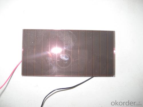
Solar Silicon Wafer - Amorphous Silicon Dice Specification 4
- Ref Price:
-

- Loading Port:
- China Main Port
- Payment Terms:
- TT OR LC
- Min Order Qty:
- -
- Supply Capability:
- -
OKorder Service Pledge
OKorder Financial Service
You Might Also Like


Pv modules at present, the mainstream products are still in silicon as the main raw materials, only in terms of silicon raw material consumption, production 1 mw of crystalline silicon solar cell, need 10 to 12 tons of high purity silicon, but if use the same silicon materials used to produce thin film amorphous silicon solar cell can produce more than 200 mw.
From the perspective of energy consumption, amorphous silicon solar battery only 1-1.5 years of energy recovery period, more embodies its contribution to energy saving in the manufacturing process.
Component occupies a high proportion of costs in a photovoltaic system, the component prices directly affect the system cost, and thus affect the cost of photovoltaic power generation. Calculated at the current price of components, the same money, buy amorphous silicon products, you can get more close to 30% of the power components.
2, more power
For the same power of solar cell array, amorphous silicon solar cell is about 10% more than monocrystalline silicon, polycrystalline silicon battery power. This has been the Uni - Solar System LLC, Energy Photovoltaic Corp., Japan's Kaneka Corp., the Netherlands Energy research institute, and other organizations and experts confirmed that the Photovoltaic industry.
In sunny, that is to say, under the high temperature, amorphous silicon solar cell components can show more excellent power performance.
3, better low light response
Due to the characteristics of amorphous silicon atoms are arranged disorderly, the electron transition no longer comply with the restriction of traditional \"selection rule\", as a result, its light absorption characteristics and there are big differences monocrystalline silicon material. Amorphous silicon and monocrystalline silicon material absorption curve as shown
, amorphous silicon absorption curve has obvious three sections (A, B, C). Area A corresponding electronic transition between localized states, such as the gap state near Fermi level and to the tail state transition, the absorption coefficient is small, about 1-10 cm - 1, for this is absorbing; B area absorption coefficient with the increase of the photon energy index rose, it corresponds to the electrons from the valence band edge extension state to the conduction band localized state transition, as well as the localized electrons from the valence band tail states guide for edge extension state transition, the region's energy range is usually only about half of the electron volts, but absorption coefficient across two or three orders of magnitude, usually up to 104 cm - 1; Area C corresponds to the electrons from the valence band to the conduction band internal internal transition, the absorption coefficient is bigger, often in more than 104 cm - 1. After two absorption area is crystalline silicon eigen absorption area.
Can be seen in the figure, the intersection of two curves about 1.8 ev. It is important to note that in the visible light range (1.7 to 3.0 ev), the absorption coefficient of amorphous silicon material is almost an order of magnitude larger than the single crystal silicon. That is to say, in the morning the first part of the sun is not too strong, the second half, and it's cloudy in the afternoon under the condition of low light intensity, long wave is greater, the amorphous silicon material still has a large absorption coefficient. Again considering the amorphous silicon band gap is larger, the reverse saturation current I0 is smaller. And as mentioned the amorphous silicon battery the characteristics I - V characteristic curve of the amorphous silicon solar cell both in theory and in practical use in low light intensity has good adaptation.
• I - V characteristics of amorphous silicon cells after more than a Vm with the voltage drop slowly
In order to be convenient, we draw the I - V characteristics of two kinds of batteries on the same picture. Crystalline silicon and amorphous silicon battery I - V characteristics of general shape as shown
we see from the picture, two kinds of cells in the curve changes after exceed the maximum output power point gap is bigger. Output current of crystalline silicon cells after exceed the maximum output power point will soon fall to zero, curve steep; Rather than crystalline silicon cells output current after a long distance to fall to zero, the curve is relatively flat. Two kinds of battery Vm equivalent to about 83% of its open circuit voltage and 83% respectively.
when light intensity gradually become hour, short circuit current and open circuit voltage of solar battery will be stronger. Short circuit current decreases faster, of course, open circuit voltage decrease more slowly.
do in battery solar cell array under the condition of load, when the sun battery array of effective output voltage less than the terminal voltage of battery, battery cannot be recharged. When the light intensity gradually become hour, crystal silicon battery charging does not meet the conditions, and amorphous silicon due to the larger voltage difference, do not charge until the light is very dark, effectively increase the use of sunlight time. So, amorphous silicon cells to produce more electricity than the crystalline silicon.
4, more excellent high temperature performance
High in the outdoor environment temperature, amorphous silicon solar cell performance change, depends on the temperature, spectrum, as well as other related factors. But what is certain is: amorphous silicon than monocrystalline silicon or polycrystalline silicon are less likely to be affected by temperature.
Amorphous silicon solar cells than monocrystalline silicon, polycrystalline silicon cells have relatively small temperature coefficient of amorphous silicon solar cell output power best Pm temperature coefficient is about 0.19%, and monocrystalline silicon, polycrystalline silicon cells best output power Pm temperature coefficient is about 0.5%, when the battery work at higher temperatures, the two batteries will be a drop in the Pm, but the decline is different. They can be calculated using the following formula.
- Q: What is the role of a bypass diode in a solar silicon wafer?
- The role of a bypass diode in a solar silicon wafer is to provide an alternate pathway for the flow of current in case of shading or malfunctioning of individual solar cells. This helps prevent power loss and damage to the entire solar panel by allowing the unaffected cells to continue generating electricity.
- Q: What is the efficiency of a solar cell made with silicon wafers?
- The efficiency of a solar cell made with silicon wafers can vary, but on average, it ranges from 15% to 25%.
- Q: What is the expected cost reduction for solar silicon wafers in the future?
- It is difficult to provide an exact figure for the expected cost reduction of solar silicon wafers in the future as it depends on various factors such as technological advancements, economies of scale, and market demand. However, with ongoing research and development efforts in the solar industry, it is anticipated that the cost of silicon wafers will continue to decrease over time, making solar energy more affordable and accessible for consumers and businesses alike.
- Q: How is a glass cover attached to a solar silicon wafer?
- A glass cover is typically attached to a solar silicon wafer using a specialized adhesive or encapsulant material. This material is applied between the glass cover and the wafer, creating a strong bond that ensures the cover stays securely in place. Additionally, the adhesive or encapsulant also provides protection against moisture, dust, and other environmental factors, safeguarding the delicate solar cells within the wafer.
- Q: How is a passivation layer applied to a solar silicon wafer?
- A passivation layer is typically applied to a solar silicon wafer through a process called chemical passivation. This involves immersing the wafer in a solution containing chemicals that help remove impurities and contaminants from the surface. The chemicals react with the wafer, forming a thin layer of passivation material that acts as a protective barrier against further oxidation and degradation. This passivation layer enhances the efficiency and lifespan of the solar cell.
- Q: What's the connection between silicon wafer and wafer
- The bigger the chip the smaller the less waste the less the cost. His direct use is of course on Si for mixed metal precipitation until different packaging lithography, as raw materials for the preparation of electronic manufacturing
- Q: What is the role of a back surface field in a solar silicon wafer?
- The role of a back surface field in a solar silicon wafer is to enhance the efficiency of the solar cell by reducing the recombination of charge carriers at the back surface. It accomplishes this by creating a high-quality passivation layer that prevents the loss of carriers, thus increasing the overall performance of the solar cell.
- Q: Can solar silicon wafers be used in agricultural applications?
- Yes, solar silicon wafers can be used in agricultural applications. They can be integrated into solar panels to generate renewable electricity for various agricultural tasks, such as powering irrigation systems, livestock water pumps, or even electric fences. Additionally, solar technology can be utilized in greenhouses to provide supplemental lighting or heating, enhancing crop growth and productivity.
- Q: Are there any limitations to the size of solar silicon wafers?
- Yes, there are limitations to the size of solar silicon wafers. Currently, the most common size for solar silicon wafers is around 156 mm x 156 mm or 6 inches x 6 inches. This size is widely used in the solar industry due to various factors such as manufacturing capabilities, handling, and compatibility with existing solar cell production equipment. However, larger wafer sizes, such as 166 mm x 166 mm or even larger, are being developed and implemented to increase solar panel efficiency and reduce manufacturing costs. Nonetheless, there are practical limitations to the size of solar silicon wafers, including the challenges related to handling larger sizes, potential increase in material waste, and compatibility with existing solar panel designs and installations.
- Q: How do solar silicon wafers contribute to the overall weight of a solar panel?
- Solar silicon wafers contribute significantly to the overall weight of a solar panel. These wafers are the primary material used to convert sunlight into electricity. Since solar panels consist of multiple layers of silicon wafers, they account for a substantial portion of the panel's weight. The thickness and number of wafers used determine the weight, and while efforts have been made to reduce their thickness to minimize weight, they remain a significant factor in determining the overall weight of a solar panel.
Send your message to us
Solar Silicon Wafer - Amorphous Silicon Dice Specification 4
- Ref Price:
-
- Loading Port:
- China Main Port
- Payment Terms:
- TT OR LC
- Min Order Qty:
- -
- Supply Capability:
- -
OKorder Service Pledge
OKorder Financial Service
Similar products


Hot products


Hot Searches
Related keywords

