


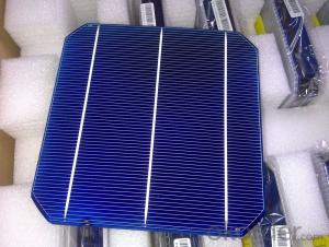
Solar Silicon Wafer for Sale - High Quality A Grade Monocrystalline 5V 19.2% Solar Cell
- Ref Price:
-

- Loading Port:
- Shanghai
- Payment Terms:
- TT OR LC
- Min Order Qty:
- 1000 pc
- Supply Capability:
- 100000 pc/month
OKorder Service Pledge
OKorder Financial Service
You Might Also Like


Specifications
hot sale solar cell
1.16.8%~18.25% high efficiency
2.100% checked quality
3.ISO9001/ISO14001/TUV/CE/UL
4.stable performance
We can offer you the best quality products and services, don't miss !
POLY6'(156*156)
Polycrystalline Silicon Solar cell
Physical Characteristics
Dimension: 156mm×156mm±0.5mm
Diagonal: 220mm±0.5mm
Thickness(Si): 200±20 μm
Front(-) Back(+)
Blue anti-reflecting coating (silicon nitride); Aluminum back surface field;
1.5mm wide bus bars; 2.0mm wide soldering pads;
Distance between bus bars: 51mm . Distance between bus bars :51mm .
Electrical Characteristics
Efficiency(%) | 18.00 | 17.80 | 17.60 | 17.40 | 17.20 | 16.80 | 16.60 | 16.40 | 16.20 | 16.00 | 15.80 | 15.60 |
Pmpp(W) | 4.33 | 4.29 | 4.24 | 4.19 | 4.14 | 4.09 | 4.04 | 3.99 | 3.94 | 3.90 | 3.86 | 3.82 |
Umpp(V) | 0.530 | 0.527 | 0.524 | 0.521 | 0.518 | 0.516 | 0.514 | 0.511 | 0.509 | 0.506 | 0.503 | 0.501 |
Impp(A) | 8.159 | 8.126 | 8.081 | 8.035 | 7.990 | 7.938 | 7.876 | 7.813 | 7.754 | 7.698 | 7.642 | 7.586 |
Uoc(V) | 0.633 | 0.631 | 0.628 | 0.625 | 0.623 | 0.620 | 0.618 | 0.617 | 0.615 | 0.613 | 0.611 | 0.609 |
Isc(A) | 8.709 | 8.677 | 8.629 | 8.578 | 8.531 | 8.478 | 8.419 | 8.356 | 8.289 | 8.220 | 8.151 | 8.083 |

MONO5'(125*125mm)165
Monocrystalline silicon solar cell
Physical Characteristics
Dimension: 125mm×125mm±0.5mm
Diagonal: 165mm±0.5mm
Thickness(Si): 200±20 μm
Front(-) Back(+)
Blue anti-reflecting coating(silicon nitride); Aluminum back surface field;
1.6mmwide bus bars; 2.5mm wide soldering pads;
Distance between bus bars: 61mm . Distance between bus bars :61mm .
Electrical Characteristics
Efficiency(%) | 19.40 | 19.20 | 19.00 | 18.80 | 18.60 | 18.40 | 18.20 | 18.00 | 17.80 | 17.60 | 17.40 | 17.20 |
Pmpp(W) | 2.97 | 2.94 | 2.91 | 2.88 | 2.85 | 2.82 | 2.79 | 2.76 | 2.73 | 2.70 | 2.67 | 2.62 |
Umpp(V) | 0.537 | 0.535 | 0.533 | 0.531 | 0.527 | 0.524 | 0.521 | 0.518 | 0.516 | 0.515 | 0.513 | 0.509 |
Impp(A) | 5.531 | 5.495 | 5.460 | 5.424 | 5.408 | 5.382 | 5.355 | 5.328 | 5.291 | 5.243 | 5.195 | 4.147 |
Uoc(V) | 0.637 | 0.637 | 0.636 | 0.635 | 0.633 | 0.630 | 0.629 | 0.629 | 0.628 | 0.626 | 0.626 | 0.625 |
Isc(A) | 5.888 | 5.876 | 5.862 | 5.848 | 5.839 | 5.826 | 5.809 | 5.791 | 5.779 | 5.756 | 5.293 | 5.144 |

FAQ:
Q:How can i get some sample?
A:Yes , if you want order ,sample is not a problem.
Q:How about your solar panel efficency?
A: Our product efficency around 17.25%~18.25%.
Q:What’s the certificate you have got?
A: we have overall product certificate of ISO9001/ISO14001/CE/TUV/UL
- Q: What is the weight of a solar silicon wafer?
- The weight of a solar silicon wafer can vary depending on its size and thickness. On average, a standard solar silicon wafer weighs around 2-4 grams.
- Q: Can solar silicon wafers be used in harsh climates?
- Yes, solar silicon wafers can be used in harsh climates. They are designed to withstand various environmental conditions, including extreme temperatures, humidity, and even exposure to dust and sand. Additionally, solar panels are tested and certified to ensure their durability and performance in harsh climates, making them suitable for use in such environments.
- Q: What are the advantages of using a solar silicon wafer?
- There are several advantages of using a solar silicon wafer. Firstly, silicon wafers have high efficiency in converting sunlight into electricity, making them ideal for solar panel production. Secondly, silicon is abundant and widely available, ensuring a stable supply for solar industry growth. Additionally, silicon wafers have a long lifespan, typically lasting for over 25 years, resulting in cost-effectiveness over time. Lastly, silicon wafers are relatively easy to manufacture and handle, facilitating mass production and installation of solar panels.
- Q: What are the different manufacturing processes for solar silicon wafers?
- There are mainly two manufacturing processes for solar silicon wafers: the Czochralski (CZ) process and the Float Zone (FZ) process. In the CZ process, a silicon crystal is grown from a molten silicon melt using a seed crystal, which is then sliced into wafers. The FZ process involves slowly pulling a silicon crystal through a molten zone, creating a solid silicon cylinder that is then sliced into wafers. Both processes require further steps such as wafer polishing and cleaning to produce high-quality solar silicon wafers.
- Q: What is the purpose of a fill factor in a solar silicon wafer?
- The purpose of a fill factor in a solar silicon wafer is to measure the efficiency of the solar cell. It represents the ratio of the actual power output of the cell to the maximum possible power output, taking into account the cell's open circuit voltage and short circuit current. A higher fill factor indicates a more efficient solar cell, demonstrating how effectively it converts sunlight into electricity.
- Q: Are solar silicon wafers affected by power grid fluctuations?
- No, solar silicon wafers are not directly affected by power grid fluctuations. Solar panels generate electricity independently of the power grid, using sunlight to produce energy. However, fluctuations in the power grid can indirectly impact the overall efficiency and performance of solar panels, as they rely on a stable grid connection for grid-tied systems or for energy storage purposes.
- Q: How do solar silicon wafers handle temperature variations?
- Solar silicon wafers are designed to handle temperature variations quite well. They have a low coefficient of thermal expansion, which means they can expand and contract without being damaged. The materials used in their construction are highly stable and can withstand a wide range of temperatures, from extreme heat to freezing cold. This resilience allows solar silicon wafers to efficiently convert sunlight into electricity regardless of the surrounding temperature.
- Q: Are solar silicon wafers affected by snow or ice accumulation?
- Yes, solar silicon wafers can be affected by snow or ice accumulation. Snow or ice covering the surface of the solar panels can block sunlight from reaching the silicon wafers, reducing their efficiency and power output. Regular removal of snow or ice from the panels is recommended to ensure optimal performance.
- Q: Can solar silicon wafers be used in solar-powered security systems?
- Yes, solar silicon wafers can be used in solar-powered security systems. These wafers are commonly used in the production of solar cells, which convert sunlight into electricity. By harnessing solar energy, security systems can operate independently, without relying on grid power or batteries. Solar silicon wafers provide a reliable and sustainable solution for powering security systems, ensuring continuous surveillance even in remote or off-grid locations.
- Q: Can solar silicon wafers be used in portable solar chargers?
- Yes, solar silicon wafers can be used in portable solar chargers. These wafers are commonly used in the production of solar cells, which are the key component of solar chargers. The silicon wafers help convert sunlight into electricity, making them an essential part of portable solar chargers that harness solar energy to charge devices on the go.
Send your message to us
Solar Silicon Wafer for Sale - High Quality A Grade Monocrystalline 5V 19.2% Solar Cell
- Ref Price:
-
- Loading Port:
- Shanghai
- Payment Terms:
- TT OR LC
- Min Order Qty:
- 1000 pc
- Supply Capability:
- 100000 pc/month
OKorder Service Pledge
OKorder Financial Service
Similar products


Hot products


Hot Searches
Related keywords

