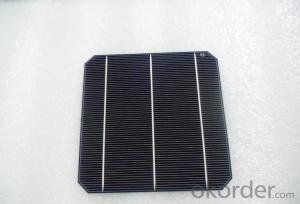


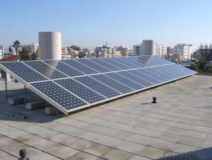
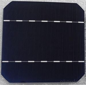
Silicone Wafer Solar Panel - High Quality A Grade Monocrystalline Solar Cell 5V 17.4%
- Ref Price:
-

- Loading Port:
- Shanghai
- Payment Terms:
- TT OR LC
- Min Order Qty:
- 1000 pc
- Supply Capability:
- 100000 pc/month
OKorder Service Pledge
OKorder Financial Service
You Might Also Like


Specifications
hot sale solar cell
1.16.8%~18.25% high efficiency
2.100% checked quality
3.ISO9001/ISO14001/TUV/CE/UL
4.stable performance
We can offer you the best quality products and services, don't miss !
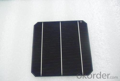
POLY6'(156*156)
Polycrystalline Silicon Solar cell
Physical Characteristics
Dimension: 156mm×156mm±0.5mm
Diagonal: 220mm±0.5mm
Thickness(Si): 200±20 μm
Front(-) Back(+)
Blue anti-reflecting coating (silicon nitride); Aluminum back surface field;
1.5mm wide bus bars; 2.0mm wide soldering pads;
Distance between bus bars: 51mm . Distance between bus bars :51mm .
Electrical Characteristics
Efficiency(%) | 18.00 | 17.80 | 17.60 | 17.40 | 17.20 | 16.80 | 16.60 | 16.40 | 16.20 | 16.00 | 15.80 | 15.60 |
Pmpp(W) | 4.33 | 4.29 | 4.24 | 4.19 | 4.14 | 4.09 | 4.04 | 3.99 | 3.94 | 3.90 | 3.86 | 3.82 |
Umpp(V) | 0.530 | 0.527 | 0.524 | 0.521 | 0.518 | 0.516 | 0.514 | 0.511 | 0.509 | 0.506 | 0.503 | 0.501 |
Impp(A) | 8.159 | 8.126 | 8.081 | 8.035 | 7.990 | 7.938 | 7.876 | 7.813 | 7.754 | 7.698 | 7.642 | 7.586 |
Uoc(V) | 0.633 | 0.631 | 0.628 | 0.625 | 0.623 | 0.620 | 0.618 | 0.617 | 0.615 | 0.613 | 0.611 | 0.609 |
Isc(A) | 8.709 | 8.677 | 8.629 | 8.578 | 8.531 | 8.478 | 8.419 | 8.356 | 8.289 | 8.220 | 8.151 | 8.083 |

MONO5'(125*125mm)165
Monocrystalline silicon solar cell
Physical Characteristics
Dimension: 125mm×125mm±0.5mm
Diagonal: 165mm±0.5mm
Thickness(Si): 200±20 μm
Front(-) Back(+)
Blue anti-reflecting coating(silicon nitride); Aluminum back surface field;
1.6mmwide bus bars; 2.5mm wide soldering pads;
Distance between bus bars: 61mm . Distance between bus bars :61mm .
Electrical Characteristics
Efficiency(%) | 19.40 | 19.20 | 19.00 | 18.80 | 18.60 | 18.40 | 18.20 | 18.00 | 17.80 | 17.60 | 17.40 | 17.20 |
Pmpp(W) | 2.97 | 2.94 | 2.91 | 2.88 | 2.85 | 2.82 | 2.79 | 2.76 | 2.73 | 2.70 | 2.67 | 2.62 |
Umpp(V) | 0.537 | 0.535 | 0.533 | 0.531 | 0.527 | 0.524 | 0.521 | 0.518 | 0.516 | 0.515 | 0.513 | 0.509 |
Impp(A) | 5.531 | 5.495 | 5.460 | 5.424 | 5.408 | 5.382 | 5.355 | 5.328 | 5.291 | 5.243 | 5.195 | 4.147 |
Uoc(V) | 0.637 | 0.637 | 0.636 | 0.635 | 0.633 | 0.630 | 0.629 | 0.629 | 0.628 | 0.626 | 0.626 | 0.625 |
Isc(A) | 5.888 | 5.876 | 5.862 | 5.848 | 5.839 | 5.826 | 5.809 | 5.791 | 5.779 | 5.756 | 5.293 | 5.144 |

FAQ:
Q:How can i get some sample?
A:Yes , if you want order ,sample is not a problem.
Q:How about your solar panel efficency?
A: Our product efficency around 17.25%~18.25%.
Q:What’s the certificate you have got?
A: we have overall product certificate of ISO9001/ISO14001/CE/TUV/UL
- Q: What is the expected efficiency improvement for tandem solar silicon wafers?
- The expected efficiency improvement for tandem solar silicon wafers is typically around 30% or more compared to single-junction solar cells.
- Q: How is a mounting structure attached to a solar silicon wafer?
- A mounting structure is typically attached to a solar silicon wafer using a combination of adhesive materials and mechanical fasteners. The adhesive material, such as a specialized bonding agent or thermal conductive paste, helps to securely bond the mounting structure to the wafer's surface. Additionally, mechanical fasteners like screws or clips are used to provide additional stability and ensure a strong attachment between the mounting structure and the silicon wafer.
- Q: Why should the wafer cut side, cut out edge Jiaosha
- To determine the crystal, cutting the adhesive carbon or glass, mounted on the fixed equipment.In simple terms is to determine the crystal direction, in order to facilitate future cutting, design graphics to consider this point, and then ask a little deeper, it is necessary to look at the book.Transistors in general with 111 sides, MOS general 110The reason for this is related to doping, corrosion and other post production, but also the activity of different layers of electrons is different, potential energy is not the same.
- Q: How do solar silicon wafers perform in high humidity environments?
- Solar silicon wafers generally perform well in high humidity environments. However, prolonged exposure to high humidity may cause a slight decrease in their efficiency over time due to increased moisture absorption. Manufacturers typically apply protective coatings or encapsulation materials to mitigate any potential degradation. Overall, while solar silicon wafers can withstand high humidity, proper maintenance and protection are important to ensure their optimal performance and longevity.
- Q: What is the difference between silicon wafer P111 and P100
- Crystal growth direction<111><100><110>The coordinate system is set up in the crystal cell
- Q: What is the maximum temperature a solar silicon wafer can handle?
- The maximum temperature that a solar silicon wafer can handle typically ranges between 200 to 300 degrees Celsius.
- Q: What is the production capacity of solar silicon wafers worldwide?
- As of 2021, the global production capacity of solar silicon wafers is estimated to be around 200 gigawatts (GW) per year.
- Q: How is the power output of a solar silicon wafer measured?
- The power output of a solar silicon wafer is typically measured by subjecting it to a controlled light source and measuring the electrical current produced by the wafer. This can be done using specialized equipment called solar simulators, which provide a calibrated light intensity similar to sunlight. The current generated by the wafer is then measured using a current-voltage (IV) curve tracer or a digital multimeter. Additionally, voltage and resistance measurements may also be recorded to calculate the power output of the solar silicon wafer using the formula P = IV, where P is power, I is current, and V is voltage.
- Q: Can solar silicon wafers be used in underwater solar energy systems?
- Yes, solar silicon wafers can be used in underwater solar energy systems. However, special considerations need to be taken into account to ensure their effectiveness and longevity in underwater environments.
- Q: Below what the photovoltaic industry specific industry classification, solar silicon manufacturing enterprises, mainly engaged in single and polycrystalline silicon, polycrystalline silicon wafer cutting casting, single enterprise, what are the concrete classification, a solar silicon slice of this industry?
- There is no specific classificationPhotovoltaic industry can be divided into the upper and middle reaches of the upper reaches of the main silicon material, silicon products, the middle reaches of the main battery, components, the lower reaches of photovoltaic power generation
Send your message to us
Silicone Wafer Solar Panel - High Quality A Grade Monocrystalline Solar Cell 5V 17.4%
- Ref Price:
-
- Loading Port:
- Shanghai
- Payment Terms:
- TT OR LC
- Min Order Qty:
- 1000 pc
- Supply Capability:
- 100000 pc/month
OKorder Service Pledge
OKorder Financial Service
Similar products


Hot products


Hot Searches
Related keywords

