


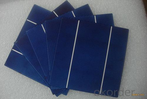


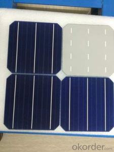
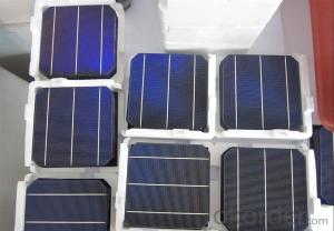
Solar Grade Silicon Wafer - High Quality A Grade Polycrystalline 5V 17.4% Solar Cell
- Ref Price:
-

- Loading Port:
- Shanghai
- Payment Terms:
- TT OR LC
- Min Order Qty:
- 1000 pc
- Supply Capability:
- 100000 pc/month
OKorder Service Pledge
OKorder Financial Service
You Might Also Like


Specifications
hot sale solar cell
1.16.8%~18.25% high efficiency
2.100% checked quality
3.ISO9001/ISO14001/TUV/CE/UL
4.stable performance
We can offer you the best quality products and services, don't miss !
POLY6'(156*156)
Polycrystalline Silicon Solar cell
Physical Characteristics
Dimension: 156mm×156mm±0.5mm
Diagonal: 220mm±0.5mm
Thickness(Si): 200±20 μm
Front(-) Back(+)
Blue anti-reflecting coating (silicon nitride); Aluminum back surface field;
1.5mm wide bus bars; 2.0mm wide soldering pads;
Distance between bus bars: 51mm . Distance between bus bars :51mm .
Electrical Characteristics
Efficiency(%) | 18.00 | 17.80 | 17.60 | 17.40 | 17.20 | 16.80 | 16.60 | 16.40 | 16.20 | 16.00 | 15.80 | 15.60 |
Pmpp(W) | 4.33 | 4.29 | 4.24 | 4.19 | 4.14 | 4.09 | 4.04 | 3.99 | 3.94 | 3.90 | 3.86 | 3.82 |
Umpp(V) | 0.530 | 0.527 | 0.524 | 0.521 | 0.518 | 0.516 | 0.514 | 0.511 | 0.509 | 0.506 | 0.503 | 0.501 |
Impp(A) | 8.159 | 8.126 | 8.081 | 8.035 | 7.990 | 7.938 | 7.876 | 7.813 | 7.754 | 7.698 | 7.642 | 7.586 |
Uoc(V) | 0.633 | 0.631 | 0.628 | 0.625 | 0.623 | 0.620 | 0.618 | 0.617 | 0.615 | 0.613 | 0.611 | 0.609 |
Isc(A) | 8.709 | 8.677 | 8.629 | 8.578 | 8.531 | 8.478 | 8.419 | 8.356 | 8.289 | 8.220 | 8.151 | 8.083 |

MONO5'(125*125mm)165
Monocrystalline silicon solar cell
Physical Characteristics
Dimension: 125mm×125mm±0.5mm
Diagonal: 165mm±0.5mm
Thickness(Si): 200±20 μm
Front(-) Back(+)
Blue anti-reflecting coating(silicon nitride); Aluminum back surface field;
1.6mmwide bus bars; 2.5mm wide soldering pads;
Distance between bus bars: 61mm . Distance between bus bars :61mm .
Electrical Characteristics
Efficiency(%) | 19.40 | 19.20 | 19.00 | 18.80 | 18.60 | 18.40 | 18.20 | 18.00 | 17.80 | 17.60 | 17.40 | 17.20 |
Pmpp(W) | 2.97 | 2.94 | 2.91 | 2.88 | 2.85 | 2.82 | 2.79 | 2.76 | 2.73 | 2.70 | 2.67 | 2.62 |
Umpp(V) | 0.537 | 0.535 | 0.533 | 0.531 | 0.527 | 0.524 | 0.521 | 0.518 | 0.516 | 0.515 | 0.513 | 0.509 |
Impp(A) | 5.531 | 5.495 | 5.460 | 5.424 | 5.408 | 5.382 | 5.355 | 5.328 | 5.291 | 5.243 | 5.195 | 4.147 |
Uoc(V) | 0.637 | 0.637 | 0.636 | 0.635 | 0.633 | 0.630 | 0.629 | 0.629 | 0.628 | 0.626 | 0.626 | 0.625 |
Isc(A) | 5.888 | 5.876 | 5.862 | 5.848 | 5.839 | 5.826 | 5.809 | 5.791 | 5.779 | 5.756 | 5.293 | 5.144 |

FAQ:
Q:How can i get some sample?
A:Yes , if you want order ,sample is not a problem.
Q:How about your solar panel efficency?
A: Our product efficency around 17.25%~18.25%.
Q:What’s the certificate you have got?
A: we have overall product certificate of ISO9001/ISO14001/CE/TUV/UL
- Q: Are solar silicon wafers affected by electromagnetic interference (EMI)?
- Yes, solar silicon wafers can be affected by electromagnetic interference (EMI). EMI refers to the disruption caused by electromagnetic fields on electronic devices, and solar silicon wafers, being electronic components used in solar panels, are not immune to this interference. EMI can potentially impact the efficiency and performance of solar panels, leading to a decrease in power output. Therefore, it is important to consider EMI mitigation techniques during the design and installation of solar systems to minimize its impact on the silicon wafers and overall solar panel performance.
- Q: What is the impact of temperature on the performance of solar silicon wafers?
- The impact of temperature on the performance of solar silicon wafers is significant. Higher temperatures generally lead to a decrease in the efficiency of solar cells, resulting in reduced power output. This is primarily due to the increased resistance within the silicon material, which leads to a higher voltage drop and lower current flow. Additionally, higher temperatures can cause an increase in the rate of electron-hole recombination, further reducing the efficiency of the solar cell. Therefore, it is crucial to manage and control the temperature to optimize the performance of solar silicon wafers and maximize their energy conversion capabilities.
- Q: How do solar silicon wafers perform in cold climates?
- Solar silicon wafers perform well in cold climates as the low temperatures actually enhance their efficiency. The cold weather helps to reduce the resistance in the solar cells, allowing them to produce more electricity. However, extreme cold can lead to issues such as snow accumulation, which may temporarily hinder their performance until cleared. Overall, solar silicon wafers are designed to withstand and operate efficiently in cold weather conditions.
- Q: Can solar silicon wafers be used in remote or isolated areas?
- Yes, solar silicon wafers can be used in remote or isolated areas. Solar panels, which incorporate silicon wafers, are a reliable and effective source of renewable energy. They can operate independently, without the need for a grid connection, making them suitable for powering remote or isolated areas where traditional power infrastructure is not available.
- Q: How are solar silicon wafers cut from a silicon ingot?
- Solar silicon wafers are typically cut from a silicon ingot using a process called wire sawing. In this method, a wire made of a hard and abrasive material, such as diamond, is used to slice through the ingot. The wire is guided by a set of pulleys and continuously fed with a slurry mixture of silicon carbide and water to aid in the cutting process. As the wire moves through the ingot, it gradually separates it into thin wafers, which can then be further processed and used in the production of solar cells.
- Q: Solar silicon wafer cutting fluid content is polyethylene glycol, flash point 182-278 DEG C, saturated vapor pressure of 6.21KPa/20 C / C in storage in the barrel, after exposure, its volatile gas is harmful?
- Silicon in a weak base and water will slowly release hydrogen
- Q: How do solar silicon wafers contribute to reducing air pollution?
- Solar silicon wafers contribute to reducing air pollution by enabling the production of clean and renewable energy. When sunlight hits the silicon wafers, it generates electricity without any harmful emissions or pollution. By replacing traditional fossil fuel-based energy sources with solar power, we can reduce the reliance on coal, oil, and gas, which are major contributors to air pollution.
- Q: What are the different types of anti-reflective coatings used on solar silicon wafers?
- There are primarily two types of anti-reflective coatings used on solar silicon wafers: silicon nitride (SiNx) and titanium dioxide (TiO2). These coatings are applied to minimize reflection and increase the absorption of sunlight, thereby enhancing the efficiency of solar cells. SiNx coatings are commonly used due to their excellent optical properties and compatibility with silicon wafers. TiO2 coatings, on the other hand, offer high refractive index and can be used in conjunction with SiNx to further reduce reflection and improve light trapping within the solar cells.
- Q: How are solar silicon wafers etched to enhance light absorption?
- Solar silicon wafers are etched to enhance light absorption by using a chemical process called texturization. In this process, a mixture of acids is applied to the surface of the wafers, which creates tiny pyramid-like structures. These structures help to scatter and trap light within the material, increasing the chances of its absorption. This etching technique, known as black silicon, significantly improves the efficiency of solar cells by maximizing light absorption and reducing reflection.
- Q: Can solar silicon wafers be used in solar-powered electric vehicles?
- Yes, solar silicon wafers can be used in solar-powered electric vehicles. These wafers are typically used in photovoltaic (PV) solar panels to convert sunlight into electricity. By integrating solar panels made of silicon wafers onto the surface of a solar-powered electric vehicle, it can generate electricity from the sun and contribute to powering the vehicle. However, the efficiency and power output of the solar panels depend on various factors such as the size of the panels, the quality of the silicon wafers, and the amount of sunlight available.
Send your message to us
Solar Grade Silicon Wafer - High Quality A Grade Polycrystalline 5V 17.4% Solar Cell
- Ref Price:
-
- Loading Port:
- Shanghai
- Payment Terms:
- TT OR LC
- Min Order Qty:
- 1000 pc
- Supply Capability:
- 100000 pc/month
OKorder Service Pledge
OKorder Financial Service
Similar products


Hot products


Hot Searches
Related keywords

