
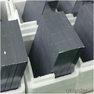

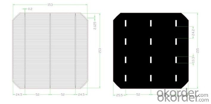

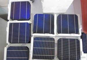
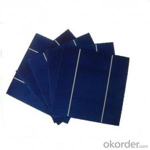
Silicon Wafer Solar Cell - 4w S Grade 156.75*156.75mm Polycrystalline Solar Cell
- Ref Price:
-

- Loading Port:
- China main port
- Payment Terms:
- TT or LC
- Min Order Qty:
- 100 watt
- Supply Capability:
- 10000 watt/month
OKorder Service Pledge
OKorder Financial Service
You Might Also Like


4W A Grade 156.75*156.75mm Polycrystalline Solar Cell
Solar Module Summarize
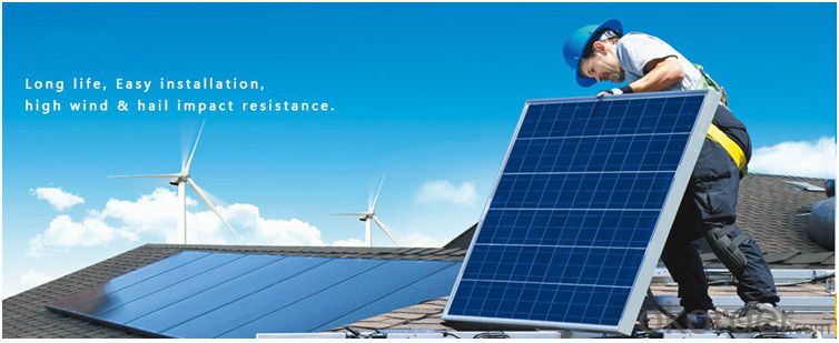
Solar Module is the core part of solar PV power systems,also is the highest value part of it. The function of Solor Module is to convert the sun's radiation to electrical energy, or transfer it to battery and store in it, or to drive the load running.
The Product has been widely used in space and ground, it mainly used for power generation systems, charging systems, road lighting and traffic signs areas. It could offer a wide range of power and voltage, and with high conversion efficiency, and long service life.
Main Characteristic
Long Service Life
High Efficiency Solar Cells
Special Aluminum Frame Design
High Transmission, Low Iron Tempered Glass
Advanced Cell Encapsulation
APPLICATIONS
Solar power stations
Rural electrification, Small home power systems
Power supply for traffic, security, gas industry
12V and 24V battery charging system
Other industrial and commercial application
Typical I-V curve

Product Show


Warranties
6Inch 2BB Polycrystalline Multi Solar Cells Mono Solar Cell
For c-Si panel: 25years output warranty for no less than 80% of performance, 10 years output warranty for no less than 90% of performance. Free from material and workmanship defects within 5 years.
For a-Si panel: 20 years output warranty for no less than 80% of performance, 10 years output warranty for no less than 90% of performance. Free from material and workmanship defects within 2 years.
- Q: What is the role of solar silicon wafers in rural electrification?
- Solar silicon wafers play a crucial role in rural electrification by serving as the main component in solar panels. These wafers are responsible for converting sunlight into electrical energy through the photovoltaic effect. By harnessing solar power, rural communities can generate their own electricity, reducing their dependence on traditional energy sources and improving access to clean and sustainable energy. Solar silicon wafers enable the production of cost-effective solar panels, making solar energy an accessible and viable solution for rural electrification, ultimately contributing to economic development, improved living conditions, and environmental sustainability.
- Q: How does the efficiency of a solar silicon wafer change over time?
- The efficiency of a solar silicon wafer tends to decrease over time due to various factors such as degradation of the materials, exposure to environmental conditions, and the accumulation of dirt or debris on the surface. These factors can lead to a decrease in the wafer's ability to convert sunlight into electricity, resulting in a gradual decline in its efficiency. Regular maintenance and cleaning can help mitigate some of these effects and prolong the lifespan of the solar silicon wafer.
- Q: What is the meaning of a cleaning in a semiconductor silicon wafer process? RCA?
- () APM (SC-1): NH4OH/H2O2 /H2O 30 ~ 80 DEG C due to the action of H2O2, the surface of the silicon wafer has a natural oxide film (SiO2), which is hydrophilic, and the surface of the silicon wafer can be soaked with the cleaning liquid. Because the natural oxide layer on the surface of silicon wafer and the Si on the surface of silicon wafer are corroded by NH 4OH, the particles attached to the surface of the silicon wafer will fall into the cleaning liquid, so as to achieve the purpose of removing particles. At the same time, the H2O 2 forms a new oxide film on the surface of the oxidized silicon wafer when the NH4OH is etched on the surface of the silicon wafer.
- Q: How to convert photovoltaic silicon MW
- 1MW=100 myriabit125*125 film general single chip 2.3W--2.8W156*156 film general single chip 3.6W-4.2WSilicon chip number =100W divided by Monolithic Power
- Q: What is the impact of impurities on the durability of solar silicon wafers?
- Impurities in solar silicon wafers can have a significant impact on their durability. These impurities can affect the structural integrity and electrical properties of the wafers, leading to reduced efficiency and shorter lifespan of the solar cells. Impurities like metal ions or oxygen can introduce defects in the crystal lattice, causing degradation and increased recombination of charge carriers. This can result in reduced power output and decreased overall performance of the solar panels. Therefore, minimizing impurities and ensuring high purity silicon is crucial for enhancing the durability and longevity of solar silicon wafers.
- Q: Can solar silicon wafers be used in solar-powered medical devices?
- Yes, solar silicon wafers can be used in solar-powered medical devices. These devices can harness solar energy to power medical equipment and devices, making them more sustainable and independent from traditional power sources.
- Q: How are solar silicon wafers protected from theft or unauthorized use?
- Solar silicon wafers are typically protected from theft or unauthorized use through several measures. These measures include physical security measures such as surveillance cameras, secure storage facilities, and restricted access to manufacturing facilities. Additionally, strict inventory management processes and tracking systems are implemented to ensure the traceability and accountability of each wafer. Furthermore, many manufacturers also employ advanced anti-counterfeiting techniques like unique identifiers or holograms on the wafers, making it difficult for unauthorized use or resale. Overall, a combination of physical security measures, strict inventory management, and anti-counterfeiting techniques help safeguard solar silicon wafers from theft or unauthorized use.
- Q: What are the different manufacturing methods for solar silicon wafers?
- There are primarily three different manufacturing methods for solar silicon wafers: the Czochralski (CZ) method, the Float-Zone (FZ) method, and the Multi-Crystalline Silicon (mc-Si) method. The CZ method involves growing a single crystal ingot of silicon by slowly pulling a seed crystal from a molten silicon melt. The FZ method uses a similar technique but with a special process that eliminates impurities, resulting in higher-quality wafers. The mc-Si method, on the other hand, involves melting and solidifying multiple silicon crystals together to form a block, which is then cut into wafers. Each method has its own advantages and disadvantages in terms of cost, efficiency, and quality.
- Q: What is the impact of microcracks in solar silicon wafers on performance?
- Microcracks in solar silicon wafers can have a significant impact on the performance of solar cells. These cracks can weaken the structure of the wafer, making it more prone to breakage during handling or installation. Additionally, microcracks can impede the flow of electrical current within the solar cell, reducing its overall efficiency. This can lead to decreased power output and lower energy conversion rates, impacting the overall performance and productivity of the solar module. Therefore, addressing and minimizing microcracks in silicon wafers is crucial for optimizing the performance and longevity of solar panels.
- Q: What are the different types of solar silicon wafers?
- There are primarily three types of solar silicon wafers: monocrystalline, polycrystalline, and thin-film. Monocrystalline wafers are made from a single crystal structure, offering high efficiency but are more expensive. Polycrystalline wafers are made from multiple crystals, providing lower efficiency but at a lower cost. Thin-film wafers are made from a thin layer of semiconductor material deposited onto a substrate, offering flexibility and lower costs, but with lower efficiency compared to crystalline silicon wafers.
Send your message to us
Silicon Wafer Solar Cell - 4w S Grade 156.75*156.75mm Polycrystalline Solar Cell
- Ref Price:
-
- Loading Port:
- China main port
- Payment Terms:
- TT or LC
- Min Order Qty:
- 100 watt
- Supply Capability:
- 10000 watt/month
OKorder Service Pledge
OKorder Financial Service
Similar products


Hot products


Hot Searches

