


Wafer-Based Crystalline Silicon Solar Panels for Home Solar Power Kit 10w to 500w
- Ref Price:
-

- Loading Port:
- China main port
- Payment Terms:
- TT OR LC
- Min Order Qty:
- 500 watt
- Supply Capability:
- 20000000 watt/month
OKorder Service Pledge
OKorder Financial Service
You Might Also Like


Destription:
Solar panel refers to a panel designed to absorb the sun's rays as a source of energy for generating electricity or heating. A PV module is a packaged, connected assembly of typically 6×10 solar cells. Solar PV panels constitute the solar array of a photovoltaic system that generates and supplies solar electricity in commercial and residential applications.
Main Characteristic
1.Manufactured according to international quality and Environment Management
System (ISO9001, ISO14001)
2. By the high transmittance, low iron tempered glass, anti-aging of the EVA(polyethylene - vinyl acetate), high-performance crystalline silicon solar cells, good Weather resistance TPT (fluoroplastics composite membrane) by pyramid , has a good Weather resistance and anti-UV, hail, water-proof capacity.
3. OEM and customerized package are accepted
4. High efficiency crystalline silicon solar cells
Quality warranty
1.10 years limited warranty on material and workmanship
2. more than 90% power output in 10 years
3. more than 80% power output in 25 years
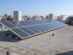
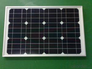
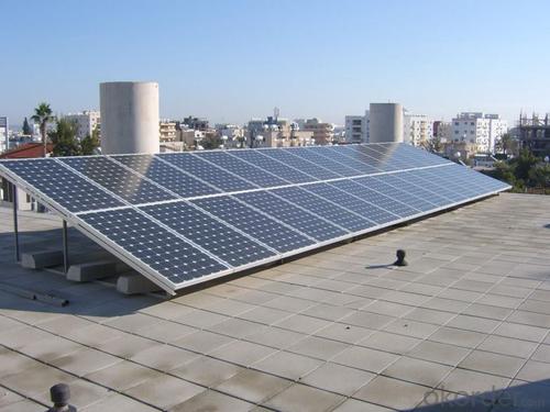
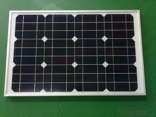
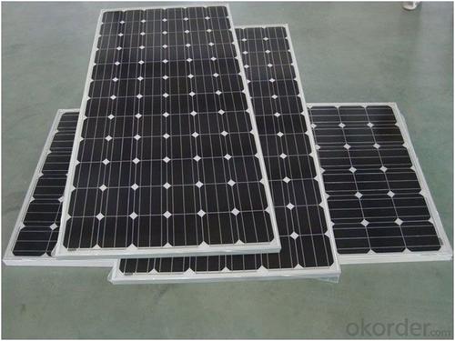
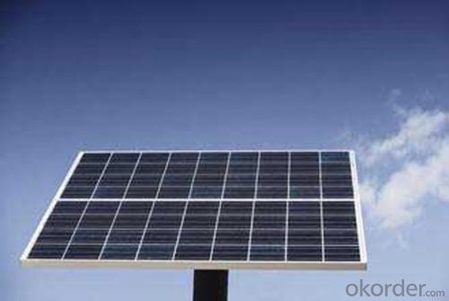
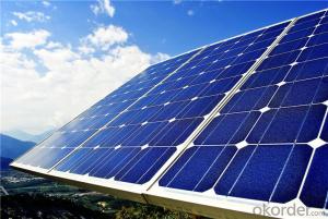
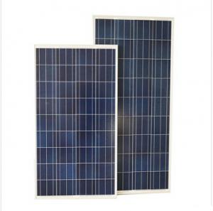
Product show


- Q: After the completion of the silicon chip will appear in the shadow of the white spots or what is the situation? How to solve. Please predecessors zhidianmijin.
- Whether or not fully diluted before drying. I couldn't see the actual product.
- Q: What is the purpose of texturing the surface of a solar silicon wafer?
- The purpose of texturing the surface of a solar silicon wafer is to increase its light absorption capability by reducing reflection. By creating a textured surface, the wafer can trap and absorb more sunlight, leading to improved efficiency and higher energy conversion in solar cells.
- Q: How are solar silicon wafers affected by light-induced annealing?
- Light-induced annealing refers to the process where solar silicon wafers are exposed to intense light, causing the defects and impurities within the material to recombine and heal. This phenomenon improves the overall quality and efficiency of the wafers, making them more effective in converting sunlight into electricity.
- Q: How does the efficiency of a solar silicon wafer change with snow cover?
- The efficiency of a solar silicon wafer decreases with snow cover. Snow acts as an insulator, preventing sunlight from reaching the wafer and reducing its ability to generate electricity. Additionally, snow can also cause shading on the surface of the wafer, further reducing its efficiency.
- Q: How does the efficiency of a solar silicon wafer change with cloud cover?
- The efficiency of a solar silicon wafer decreases with cloud cover. Solar panels rely on sunlight to generate electricity, and clouds obstruct the sunlight from reaching the panels. As a result, the reduced amount of sunlight reaching the silicon wafer leads to a decrease in its efficiency.
- Q: What is the typical shelf life of a solar silicon wafer?
- The typical shelf life of a solar silicon wafer can vary, but it is generally considered to be around 1-2 years.
- Q: Are there any alternatives to solar silicon wafers?
- Yes, there are alternatives to solar silicon wafers. Some alternative materials that can be used for solar cells include thin-film technologies such as cadmium telluride (CdTe), copper indium gallium selenide (CIGS), and organic photovoltaics (OPV). These alternatives offer different advantages and disadvantages compared to silicon wafers, such as lower production costs, flexibility, and higher efficiency in certain conditions. However, silicon wafers remain the dominant material for solar cells due to their well-established technology and high efficiency.
- Q: What is the role of a junction box sealant in a solar silicon wafer?
- The role of a junction box sealant in a solar silicon wafer is to create a protective barrier that prevents any moisture or contaminants from entering the junction box. This sealant helps maintain the integrity of the electrical connections within the junction box, ensuring the efficient and safe operation of the solar panel.
- Q: How is a degradation rate measured in a solar silicon wafer?
- The degradation rate in a solar silicon wafer is typically measured by monitoring the decrease in the efficiency or power output of the solar cell over a specific period of time. This can be done by regularly measuring the current-voltage characteristics or the maximum power point of the solar cell and comparing it to the initial performance. The degradation rate is then calculated by dividing the decrease in efficiency or power output by the duration of monitoring.
- Q: How are solar silicon wafers affected by thermal annealing?
- Solar silicon wafers are positively affected by thermal annealing. This process helps in reducing defects and impurities present in the silicon material by enhancing crystal structure and improving carrier mobility. Additionally, thermal annealing ensures better electrical conductivity and overall efficiency of the solar cells made from these wafers.
Send your message to us
Wafer-Based Crystalline Silicon Solar Panels for Home Solar Power Kit 10w to 500w
- Ref Price:
-
- Loading Port:
- China main port
- Payment Terms:
- TT OR LC
- Min Order Qty:
- 500 watt
- Supply Capability:
- 20000000 watt/month
OKorder Service Pledge
OKorder Financial Service
Similar products
Hot products


Hot Searches
Related keywords

