


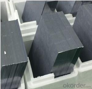
6 inch Multi Solar Silicon Wafer -- 156 x 156 mm by Solar Silicon Wafer Manufacturers
- Ref Price:
-

- Loading Port:
- China main port
- Payment Terms:
- TT OR LC
- Min Order Qty:
- 100 watt
- Supply Capability:
- 10000 watt/month
OKorder Service Pledge
OKorder Financial Service
You Might Also Like


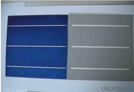
6 Inch Multi Solar Cell -- 156 x 156 mm
FEATURES
`Long Service Life
`High Efficiency Solar Cells
`Special Aluminum Frame Design
`High Transmission, Low Iron Tempered Glass
`Advanced Cell Encapsulation
Solar Module Specifications
Mono 80W—100W
Module | Type (36 Series) | |||||
Encapsulation | Glass/EVA/Cells/EVA/TPT | |||||
Parameters | SNM-M80(36) | SNM-M85(36) | SNM-M90(36) | SNM-M95(36) | SNM-M100(36) | |
Max power | Pm(W) | 80W | 85W | 90W | 95W | 100W |
Tolerance | +/-3% | |||||
Open circuit voltage | Voc(V) | 21.2 | 21.8 | 21.8 | 22.3 | 22.6 |
Short circuit current | Isc(A) | 4.84 | 5.00 | 5.30 | 5.44 | 5.68 |
Max. power voltage | Vmp(V) | 17.5 | 18.0 | 18.0 | 18.5 | 18.5 |
Max. power current | Imp(A) | 4.57 | 4.72 | 5.00 | 5.14 | 5.40 |
Dimensions | (L*W*H) | 1200x540x35mm | ||||
Net Weight | (kg) | 9 | ||||
Max. system voltage | (V) | 1000VDC | ||||
Operate Temp. Scope | -40/+85'C | |||||
Resistance | 227g steel ball fall down from 1m height and 120m/s wind | |||||
Warranty | Pm is no less 90% in 10 years and no less 80% in 25 years | |||||
STC | (Standard Test Condition: 1000W/m2, AM1.5, and 25'C) | |||||
Picture show


- Q: What are the challenges in manufacturing large-sized silicon wafers?
- One of the primary challenges in manufacturing large-sized silicon wafers is maintaining uniformity and ensuring high-quality throughout the entire wafer. As the size of the wafer increases, it becomes more difficult to control factors like crystal growth, impurities, and defects, which can impact the overall performance of the integrated circuits. Additionally, handling and processing large-sized wafers require specialized equipment and techniques, increasing the cost and complexity of the manufacturing process.
- Q: How do solar silicon wafers contribute to reducing the reliance on imported energy?
- Solar silicon wafers contribute to reducing the reliance on imported energy by enabling the production of solar panels, which generate electricity from sunlight. By harnessing the power of the sun, solar panels reduce the need for electricity generated from fossil fuels, thus decreasing the dependence on imported energy sources. Additionally, as silicon wafers are a key component in solar panel manufacturing, their production and usage promote the growth of the domestic solar industry, further reducing reliance on imported energy.
- Q: How are solar silicon wafers tested for resistivity and sheet resistance?
- Solar silicon wafers are tested for resistivity and sheet resistance using a variety of methods. One common technique is the four-point probe method, where four evenly spaced probes are placed on the surface of the wafer. A known current is passed between the outer probes, while the voltage is measured between the inner probes. By applying Ohm's law, the resistivity and sheet resistance can be calculated based on the measured current and voltage values. Another method involves using a Hall effect measurement, where a magnetic field is applied perpendicular to the wafer's surface and the resulting voltage is measured. This allows for the determination of the resistivity and sheet resistance. These testing methods help ensure the quality and performance of solar silicon wafers in photovoltaic applications.
- Q: How do solar silicon wafers perform in sandy environments?
- Solar silicon wafers perform relatively well in sandy environments due to their durability and resistance to dust and sand particles. However, excessive accumulation of sand or dust on the surface of the wafers can reduce their efficiency by blocking sunlight. Regular cleaning and maintenance are therefore necessary to ensure optimal performance in sandy conditions.
- Q: What is the role of rear surface passivation in solar silicon wafers?
- The role of rear surface passivation in solar silicon wafers is to minimize the recombination of charge carriers at the rear surface, thereby improving the efficiency of the solar cell. This passivation layer helps to reduce the losses caused by electron-hole recombination at the rear surface of the wafer, allowing more charge carriers to reach the front surface and contribute to the current generation.
- Q: How do solar silicon wafers perform in high humidity environments?
- Solar silicon wafers generally perform well in high humidity environments. However, prolonged exposure to high humidity may cause a slight decrease in their efficiency over time due to increased moisture absorption. Manufacturers typically apply protective coatings or encapsulation materials to mitigate any potential degradation. Overall, while solar silicon wafers can withstand high humidity, proper maintenance and protection are important to ensure their optimal performance and longevity.
- Q: Can solar silicon wafers be used in solar-powered educational institutions?
- Yes, solar silicon wafers can be used in solar-powered educational institutions. These wafers are a crucial component in solar panels, which are used to convert sunlight into electricity. By installing solar panels with silicon wafers, educational institutions can harness renewable energy and reduce their dependence on traditional power sources, contributing to sustainability and environmental education.
- Q: What are the different materials used for front contacts in solar silicon wafers?
- The different materials commonly used for front contacts in solar silicon wafers are typically silver (Ag) paste, aluminum (Al) paste, and copper (Cu) paste. These materials are chosen for their conductivity and ability to efficiently collect and transport the generated electricity from the solar cells.
- Q: How do solar silicon wafers contribute to job creation in the renewable energy sector?
- Solar silicon wafers contribute to job creation in the renewable energy sector by stimulating the growth of solar panel manufacturing and installation industries. The production of these wafers requires skilled labor for their fabrication, quality control, and testing processes. Additionally, the expansion of solar panel manufacturing facilities leads to job openings in various areas such as research and development, engineering, supply chain management, and sales. The demand for solar silicon wafers also drives the need for specialized technicians and installers, creating employment opportunities in the installation and maintenance of solar panels. Overall, the increasing adoption of solar silicon wafers fosters job creation across the renewable energy value chain.
- Q: What is the role of solar silicon wafers in promoting energy independence at the community level?
- Solar silicon wafers play a crucial role in promoting energy independence at the community level by serving as the key component in solar photovoltaic (PV) panels. These wafers are responsible for converting sunlight into electricity, enabling communities to generate their own clean and renewable energy. By harnessing solar power, communities can reduce their dependence on traditional fossil fuel sources, contribute to a greener environment, and potentially save on energy costs. Solar silicon wafers are instrumental in empowering communities to take control of their energy needs and contribute towards a more sustainable future.
Send your message to us
6 inch Multi Solar Silicon Wafer -- 156 x 156 mm by Solar Silicon Wafer Manufacturers
- Ref Price:
-
- Loading Port:
- China main port
- Payment Terms:
- TT OR LC
- Min Order Qty:
- 100 watt
- Supply Capability:
- 10000 watt/month
OKorder Service Pledge
OKorder Financial Service
Similar products


Hot products


Hot Searches
Related keywords

