
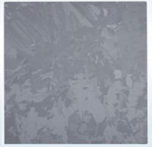

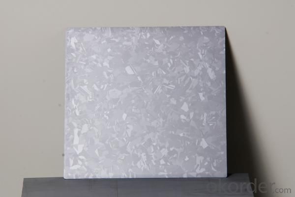


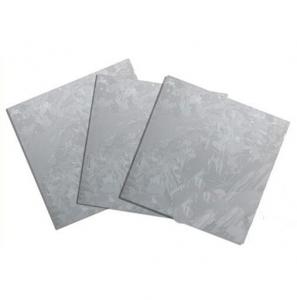
Solar Cell Silicon Wafer - Polycrystalline Solar Silicon Wafer, 125*125mm
- Ref Price:
-

- Loading Port:
- Shanghai Port
- Payment Terms:
- TT or LC
- Min Order Qty:
- 100 Pieces PCS
- Supply Capability:
- 700MW/Per Year PCS/month
OKorder Service Pledge
OKorder Financial Service
You Might Also Like


Specifications of Poly Solar Wafers
|
Product name |
Poly Wafer |
| Conductive type | P Type |
| Square size wafer (mm) | 125×125±0.5 |
| 219.20±0.5 | |
| Corner (mm)
|
1±0.5、45°±10º |
| 200±20 | |
| Total thickness(um) | ≤40 |
| Resistivity ranges(Ωcm) | 1-3 |
| Doping elements | boron |
| Carbon content(atoms/cc) | ≤8*1017 |
| Oxygen content(atoms/cc) | ≤1*1018 |
| Lifetime(μs) | ≥2 |
| Surface quality | No crack, gap, missing Angle, perforated, window, microcrystalline |
| Warping degrees(μm) | ≤50 |
| Neighbouring vertical degree | 90±0.5° |
| Side damage(mm) | ≤0.5mm(length)×0.3mm(width),(not more than 2 per wafer) |
| Line mark(μm) | ≤15 |
Advantages of Poly Solar Wafers
1. High efficiency and High power.
2. Long-term electrical stability.
3. Lowest price and Fastest delivery.
4. Good quality and good service.
5. Bulk supply
6. Good Warranty
7. Big Sale
8. More than 25 years on the lifetime.
Usage and Applications of Poly Solar Wafer
Poly Solar Wafers mainly used to make Poly Solar Cells. Our wafers are your best choice of raw material, which can greatly improve the performance of the Solar Cells and Solar Modules.
Packaging & Delivery of Poly Solar Wafer
Carton Box Package and Deliver by air. It should be noticed that it should be avoid of water, sunshine and moist.
Factory of Solar Wafers

Package Picture of Solar Wafer

- Q: What is the role of back contacts on solar silicon wafers?
- The role of back contacts on solar silicon wafers is to provide an electrical connection between the silicon wafer and the external circuitry of the solar cell. They help in collecting the generated electricity from the front surface of the cell and ensure efficient transfer of the electrical current to the external load. Additionally, back contacts also help in providing structural support to the silicon wafer, allowing for easier handling and integration into the overall solar module.
- Q: Are solar silicon wafers susceptible to cracking?
- Yes, solar silicon wafers are susceptible to cracking.
- Q: How does the temperature affect the performance of a solar silicon wafer?
- The temperature directly affects the performance of a solar silicon wafer. Higher temperatures can cause an increase in resistance within the wafer, leading to a decrease in efficiency and power output. Additionally, excessive heat can accelerate the degradation of the materials used in the wafer, reducing its lifespan. Therefore, maintaining lower temperatures is crucial for optimal performance and longevity of a solar silicon wafer.
- Q: Are solar silicon wafers affected by UV radiation?
- Yes, solar silicon wafers are affected by UV radiation. UV radiation can cause degradation and damage to the silicon material over time, reducing the efficiency and lifespan of solar panels. To mitigate this, solar panels often incorporate protective coatings or materials that can minimize the impact of UV radiation.
- Q: Can solar silicon wafers be used in underwater applications?
- No, solar silicon wafers cannot be used in underwater applications as they are not designed to withstand the harsh conditions and pressure underwater.
- Q: Can solar silicon wafers be used in mobile or portable solar chargers?
- Yes, solar silicon wafers can be used in mobile or portable solar chargers. These wafers are commonly used in the production of solar cells, which convert sunlight into electricity. By integrating solar silicon wafers into portable chargers, they can harness solar energy and charge devices on the go.
- Q: How do solar silicon wafers perform in urban environments?
- Solar silicon wafers perform well in urban environments due to their ability to efficiently convert sunlight into electricity. However, certain factors such as shading from tall buildings and pollution can impact their performance. Overall, with proper installation and maintenance, solar silicon wafers can effectively generate renewable energy even in urban settings.
- Q: How do solar silicon wafers perform in high-salt environments?
- Solar silicon wafers generally perform well in high-salt environments due to their durable and corrosion-resistant properties. The silicon material used in solar panels is typically resistant to saltwater, making them suitable for coastal areas or regions with high salt content in the air. However, it is essential to regularly clean and maintain the panels to prevent any buildup of salt deposits, which could potentially reduce their efficiency over time.
- Q: Can solar silicon wafers be made flexible for applications in wearable devices?
- Yes, solar silicon wafers can be made flexible for applications in wearable devices. Advances in technology have allowed for the development of flexible solar cells that use thin-film materials instead of rigid silicon wafers. These flexible solar cells can be integrated into wearable devices, such as smartwatches or clothing, allowing them to generate power from sunlight while maintaining their flexibility and functionality.
- Q: Below what the photovoltaic industry specific industry classification, solar silicon manufacturing enterprises, mainly engaged in single and polycrystalline silicon, polycrystalline silicon wafer cutting casting, single enterprise, what are the concrete classification, a solar silicon slice of this industry?
- There is no specific classificationPhotovoltaic industry can be divided into the upper and middle reaches of the upper reaches of the main silicon material, silicon products, the middle reaches of the main battery, components, the lower reaches of photovoltaic power generation
1. Manufacturer Overview
| Location | |
| Year Established | |
| Annual Output Value | |
| Main Markets | |
| Company Certifications |
2. Manufacturer Certificates
| a) Certification Name | |
| Range | |
| Reference | |
| Validity Period |
3. Manufacturer Capability
| a) Trade Capacity | |
| Nearest Port | |
| Export Percentage | |
| No.of Employees in Trade Department | |
| Language Spoken: | |
| b) Factory Information | |
| Factory Size: | |
| No. of Production Lines | |
| Contract Manufacturing | |
| Product Price Range | |
Send your message to us
Solar Cell Silicon Wafer - Polycrystalline Solar Silicon Wafer, 125*125mm
- Ref Price:
-
- Loading Port:
- Shanghai Port
- Payment Terms:
- TT or LC
- Min Order Qty:
- 100 Pieces PCS
- Supply Capability:
- 700MW/Per Year PCS/month
OKorder Service Pledge
OKorder Financial Service
Similar products


Hot products


Hot Searches

