


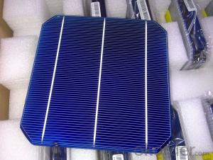
Silicon Wafer Solar Cell - High Quality A Grade Mono Crystalline 5V 18.8%
- Ref Price:
-

- Loading Port:
- Shanghai
- Payment Terms:
- TT OR LC
- Min Order Qty:
- 1000 pc
- Supply Capability:
- 100000 pc/month
OKorder Service Pledge
OKorder Financial Service
You Might Also Like


Specifications
hot sale solar cell
1.16.8%~18.25% high efficiency
2.100% checked quality
3.ISO9001/ISO14001/TUV/CE/UL
4.stable performance
We can offer you the best quality products and services, don't miss !
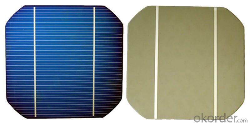
POLY6'(156*156)
Polycrystalline Silicon Solar cell
Physical Characteristics
Dimension: 156mm×156mm±0.5mm
Diagonal: 220mm±0.5mm
Thickness(Si): 200±20 μm
Front(-) Back(+)
Blue anti-reflecting coating (silicon nitride); Aluminum back surface field;
1.5mm wide bus bars; 2.0mm wide soldering pads;
Distance between bus bars: 51mm . Distance between bus bars :51mm .
Electrical Characteristics
Efficiency(%) | 18.00 | 17.80 | 17.60 | 17.40 | 17.20 | 16.80 | 16.60 | 16.40 | 16.20 | 16.00 | 15.80 | 15.60 |
Pmpp(W) | 4.33 | 4.29 | 4.24 | 4.19 | 4.14 | 4.09 | 4.04 | 3.99 | 3.94 | 3.90 | 3.86 | 3.82 |
Umpp(V) | 0.530 | 0.527 | 0.524 | 0.521 | 0.518 | 0.516 | 0.514 | 0.511 | 0.509 | 0.506 | 0.503 | 0.501 |
Impp(A) | 8.159 | 8.126 | 8.081 | 8.035 | 7.990 | 7.938 | 7.876 | 7.813 | 7.754 | 7.698 | 7.642 | 7.586 |
Uoc(V) | 0.633 | 0.631 | 0.628 | 0.625 | 0.623 | 0.620 | 0.618 | 0.617 | 0.615 | 0.613 | 0.611 | 0.609 |
Isc(A) | 8.709 | 8.677 | 8.629 | 8.578 | 8.531 | 8.478 | 8.419 | 8.356 | 8.289 | 8.220 | 8.151 | 8.083 |

MONO5'(125*125mm)165
Monocrystalline silicon solar cell
Physical Characteristics
Dimension: 125mm×125mm±0.5mm
Diagonal: 165mm±0.5mm
Thickness(Si): 200±20 μm
Front(-) Back(+)
Blue anti-reflecting coating(silicon nitride); Aluminum back surface field;
1.6mmwide bus bars; 2.5mm wide soldering pads;
Distance between bus bars: 61mm . Distance between bus bars :61mm .
Electrical Characteristics
Efficiency(%) | 19.40 | 19.20 | 19.00 | 18.80 | 18.60 | 18.40 | 18.20 | 18.00 | 17.80 | 17.60 | 17.40 | 17.20 |
Pmpp(W) | 2.97 | 2.94 | 2.91 | 2.88 | 2.85 | 2.82 | 2.79 | 2.76 | 2.73 | 2.70 | 2.67 | 2.62 |
Umpp(V) | 0.537 | 0.535 | 0.533 | 0.531 | 0.527 | 0.524 | 0.521 | 0.518 | 0.516 | 0.515 | 0.513 | 0.509 |
Impp(A) | 5.531 | 5.495 | 5.460 | 5.424 | 5.408 | 5.382 | 5.355 | 5.328 | 5.291 | 5.243 | 5.195 | 4.147 |
Uoc(V) | 0.637 | 0.637 | 0.636 | 0.635 | 0.633 | 0.630 | 0.629 | 0.629 | 0.628 | 0.626 | 0.626 | 0.625 |
Isc(A) | 5.888 | 5.876 | 5.862 | 5.848 | 5.839 | 5.826 | 5.809 | 5.791 | 5.779 | 5.756 | 5.293 | 5.144 |

FAQ:
Q:How can i get some sample?
A:Yes , if you want order ,sample is not a problem.
Q:How about your solar panel efficency?
A: Our product efficency around 17.25%~18.25%.
Q:What’s the certificate you have got?
A: we have overall product certificate of ISO9001/ISO14001/CE/TUV/UL
- Q: How does the quality of a solar silicon wafer affect solar cell performance?
- The quality of a solar silicon wafer directly impacts the performance of a solar cell. A high-quality wafer with minimal defects and impurities allows for better electron movement and higher energy conversion efficiency. It ensures optimal light absorption, reduces electron recombination, and enhances the overall performance and durability of the solar cell.
- Q: What is the expected efficiency improvement for bifacial solar silicon wafers?
- The expected efficiency improvement for bifacial solar silicon wafers can vary depending on various factors such as the technology used, manufacturing processes, and specific design of the solar module. However, on average, bifacial solar silicon wafers have shown to provide an efficiency improvement ranging from 5% to 20% compared to traditional monofacial solar panels.
- Q: How is a power output measured in a solar silicon wafer?
- A power output in a solar silicon wafer is typically measured by using a solar simulator to illuminate the wafer with a known intensity of light, and then measuring the electrical current and voltage produced by the wafer. The product of current and voltage gives the power output of the wafer.
- Q: What is the typical power output of a solar silicon wafer?
- The typical power output of a solar silicon wafer can vary depending on various factors such as the size of the wafer, the efficiency of the solar cells, and the amount of sunlight available. However, on average, a typical solar silicon wafer can produce around 4-6 watts of power per square inch.
- Q: What is the size of a typical solar silicon wafer?
- A typical solar silicon wafer is typically 156 mm (6.14 inches) in size.
- Q: What is the purpose of a junction box in a solar silicon wafer?
- The purpose of a junction box in a solar silicon wafer is to provide a secure and protective enclosure for the electrical connections between the solar cells and the external electrical system. It helps to ensure the safety and reliability of the solar panel by protecting the wiring and connections from environmental factors such as moisture, dust, and heat. Additionally, the junction box allows for easy access to the electrical connections for maintenance and troubleshooting purposes.
- Q: Why do you use a concentrated sulfuric acid and hydrogen peroxide to wash silicon?
- Because of the use of sand when the recovery of mortar used too much, resulting in increased viscosity and organic impurities
- Q: Are there any government regulations or standards for solar silicon wafers?
- Yes, there are government regulations and standards for solar silicon wafers. These regulations and standards are put in place by various governmental bodies to ensure the quality, efficiency, and safety of solar silicon wafers used in the production of solar panels. These regulations may include specifications on the purity, dimensions, chemical composition, and electrical properties of silicon wafers. Compliance with these regulations and standards is necessary for manufacturers to maintain industry standards and meet the requirements for government incentives or certifications.
- Q: Are solar silicon wafers affected by dust or dirt accumulation?
- Yes, solar silicon wafers are affected by dust or dirt accumulation. Dust and dirt can reduce the efficiency of solar panels by blocking sunlight from reaching the wafers, thereby reducing their energy output. Regular cleaning and maintenance are important to ensure optimal performance of solar panels.
- Q: Can solar silicon wafers be used in concentrated photovoltaics?
- Yes, solar silicon wafers can be used in concentrated photovoltaics (CPV). CPV systems use lenses or mirrors to concentrate a large amount of sunlight onto a small area of solar cells. While CPV typically uses multi-junction or high-efficiency solar cells, silicon wafers can also be integrated into CPV systems, although they might not be as efficient as other cell technologies specifically designed for CPV.
Send your message to us
Silicon Wafer Solar Cell - High Quality A Grade Mono Crystalline 5V 18.8%
- Ref Price:
-
- Loading Port:
- Shanghai
- Payment Terms:
- TT OR LC
- Min Order Qty:
- 1000 pc
- Supply Capability:
- 100000 pc/month
OKorder Service Pledge
OKorder Financial Service
Similar products


Hot products


Hot Searches
Related keywords

