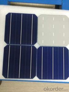

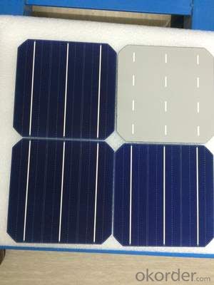


Silicon Wafer Solar Panel - Mono Solar Cells 156mm*156mm in Bulk Quantity Low Price Stock 20.0
- Ref Price:
-

- Loading Port:
- Shanghai
- Payment Terms:
- TT OR LC
- Min Order Qty:
- 1000 pc
- Supply Capability:
- 100000 pc/month
OKorder Service Pledge
OKorder Financial Service
You Might Also Like


Brief Introduction
- Up to 20.0% efficiency, one of the highest performing mono crystalline cells on the market
- Three bus bars boosts current collection over the entire cell area, leading to higher fill factors
- Blue anti-reflecting coating allows more sunlight be captured and converted to electricity
- Finer, closer fingers improves charge collections for improved energy yield
- Lower light-induced degradation leads to greater power output over the entire module lifetime
- All solar cells are tightly classified to optimize output of module
- Maximum yield and longevity due to hotspot prevention
- Premium appearance results in a highly uniform and aesthetically appealing module
Specification
- Product Mono-crystalline silicon solar cell
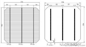
- Dimension 156 mm x 156 mm ± 0.5 mm
- Thickness 200 μm ± 30 μm
- Front 1.5 ± 0.1 mm busbar (silver)
- Silicon nitride antireflection coating
- Back 3.0 mm continuous soldering pads (silver)
- Back surface field (aluminum)
Electric performance parameters

- Testing conditions: 1000 W/m2, AM 1.5, 25 °C, Tolerance: Efficiency ± 0.2% abs., Pmpp ±1.5% rel.
- Imin : at 0.5 V
Light Intensity Dependence

Soldering Ability
- Peel Strength: > 1.0 N/mm (Pull soldered ribbon from busbar in 5 mm/s of 180°)
Dimension Figure

Quick Response
- Any time and anywhere, reply clients' email and solve all problems happen in the work at the first time.
- Remove clients doubts and offer the best solution at the first time.
- Give our clients the lastest news of the photovoltaic, update the newest stock informtion.
Production and Quality Control
- Precision cell efficiency sorting procedures
- Stringent criteria for color uniformity and appearance
- Reverse current and shunt resistance screening
- ISO9001,ISO14001 and OHSAS 18001,TUV Certificated


FAQ:
1. Q: Do you have your own factory?
A: Yes, we have. Our factory located in Jiangsu
2. Q: How can I visit your factory?
A: Before you visit,please contact us.We will show you the route or arrange a car to pick you up.
3. Q: Do you provide free sample?
A: Commenly we provide paid sample.
4. Q: Could you print our company LOGO on the nameplate and package?
A: Yes, we accept it.And need an Authorization Letter from you.
5. Q: Do you accept custom design on size?
A: Yes, if the size is reasonable.
6. Q: How can I be your agent in my country?
A: Please leave feedback. It's better for us to talk about details by email.
7. Q: Do you have solar project engineer who can guide me to install system?
A: Yes, we have a professional engineer team. They can teach you how to install a solar system.
- Q: The process for steel wire cutting silicon factory, we use HCTB5 wire, you can do?
- Electroplated diamond wireWith high tensile strength, the strength of electroplated diamond wire is more than 110% of the original strand strength. The technical problem of electroplating line embrittlement caused by plating induced tensile stress is solved successfully.
- Q: How is a junction box connector integrated into a solar silicon wafer?
- A junction box connector is integrated into a solar silicon wafer by soldering or welding it onto the metal contacts of the solar cells. This allows for the connection of multiple solar cells to form a solar panel, enabling the efficient flow of electricity generated by the cells.
- Q: How do solar silicon wafers perform in high-temperature environments?
- Solar silicon wafers generally perform well in high-temperature environments. The crystalline structure of silicon allows it to handle high temperatures without significant loss in performance. However, excessive heat can cause a slight decrease in efficiency, and prolonged exposure to extreme temperatures can result in some degradation over time. To mitigate these effects, solar panels are often designed with cooling mechanisms and protective coatings to ensure reliable performance even in hot climates.
- Q: What are the main differences between monocrystalline and polycrystalline solar silicon wafers?
- The main differences between monocrystalline and polycrystalline solar silicon wafers lie in their fabrication process and efficiency. Monocrystalline wafers are made from a single crystal structure, resulting in a uniform and pure composition. This allows them to have higher efficiency and power output, making them more suitable for applications with limited space. On the other hand, polycrystalline wafers are made from multiple crystal structures, which leads to lower efficiency and slightly lower power output. However, they are less expensive to produce and can still be effective in larger installations where space is not a constraint.
- Q: What are the different materials used for encapsulants in solar silicon wafers?
- The different materials used for encapsulants in solar silicon wafers include ethylene-vinyl acetate (EVA), polyvinyl butyral (PVB), and thermoplastic polyurethane (TPU).
- Q: Can solar silicon wafers be used in solar-powered satellites?
- Yes, solar silicon wafers can be used in solar-powered satellites. Silicon wafers are commonly used in solar panels to convert sunlight into electricity, and this technology is also applicable for powering satellites in space.
- Q: What is the role of edge isolation in solar silicon wafers?
- The role of edge isolation in solar silicon wafers is to prevent current leakage and improve overall efficiency of the solar cell. It involves removing the highly doped regions at the edges of the wafer, which helps in reducing the surface recombination and increasing the electrical isolation between adjacent solar cells. This process ensures that the current generated by the solar cell flows through the desired circuitry and minimizes any losses due to edge effects.
- Q: Are solar silicon wafers affected by vibrations or shocks?
- Yes, solar silicon wafers can be affected by vibrations or shocks. Vibrations or shocks can cause microcracks or damage to the delicate structure of the wafers, which can impact their performance and efficiency in converting sunlight into electricity. Therefore, it is important to handle and transport solar silicon wafers with care to minimize any potential damage.
- Q: What is the role of anti-reflective coatings on solar silicon wafers?
- The role of anti-reflective coatings on solar silicon wafers is to minimize reflection and maximize light absorption. These coatings help to increase the efficiency of the solar cells by reducing the amount of light that is reflected away from the surface of the wafer. By minimizing reflection, more light is able to penetrate the silicon material, leading to higher energy conversion rates and improved overall performance of the solar panel.
- Q: How is the demand for solar silicon wafers expected to grow in the future?
- The demand for solar silicon wafers is expected to grow significantly in the future due to the increasing adoption of solar energy as a sustainable and renewable source of power. As countries and industries shift towards clean energy solutions, the demand for solar panels, which heavily rely on silicon wafers, is projected to rise. Additionally, advancements in technology and manufacturing processes are likely to drive down costs, making solar power more accessible and further boosting the demand for silicon wafers.
Send your message to us
Silicon Wafer Solar Panel - Mono Solar Cells 156mm*156mm in Bulk Quantity Low Price Stock 20.0
- Ref Price:
-
- Loading Port:
- Shanghai
- Payment Terms:
- TT OR LC
- Min Order Qty:
- 1000 pc
- Supply Capability:
- 100000 pc/month
OKorder Service Pledge
OKorder Financial Service
Similar products


Hot products


Hot Searches
Related keywords

