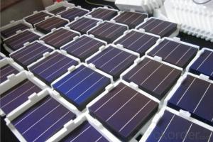


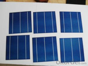
Solar Panel Silicon Wafer - High Current 16.6% Polycrystalline Silicon Solar Cell
- Ref Price:
-

- Loading Port:
- Shanghai
- Payment Terms:
- TT OR LC
- Min Order Qty:
- 1000 pc
- Supply Capability:
- 100000 pc/month
OKorder Service Pledge
OKorder Financial Service
You Might Also Like


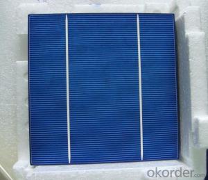
4 Bus Bars 156*156 17.6% efficiency poly solar cell
PHYSICAL CHARACTERISTICS
Dimension: 156mm x 156mm ± 0.5mm
Wafer Thickeness: 180um+20um and 200um+20um
Front(-) Four 1.2mm silver busbar
Silicon nitride blue anti-reflection coating
Back(+) aluminum back surface field
1.75mm(silver) wide segment soldering pads

Typical Electrical Characteristics
Efficiency | W(Pmpp) | V(Umpp) | A(Impp) | V(Uoc) | A(Isc) |
17.4-17.5 | 4.234 | 0.517 | 8.231 | 0.622 | 8.759 |
17.5-17.6 | 4.259 | 0.519 | 8.243 | 0.623 | 8.769 |
17.7-17.8 | 4.283 | 0.521 | 8.256 | 0.625 | 8.779 |
17.8-17.9 | 4.307 | 0.523 | 8.268 | 0.626 | 8.788 |
17.9-18.0 | 4.332 | 0.525 | 8.281 | 0.627 | 8.798 |
18.0-18.1 | 4.380 | 0.529 | 8.306 | 0.629 | 8.808 |
18.1-18.2 | 4.405 | 0.531 | 8.318 | 0.632 | 8.818 |
18.2-18.3 | 4.429 | 0.533 | 8.331 | 0.633 | 8.837 |
18.3-18.4 | 4.453 | 0.535 | 8.344 | 0.634 | 8.847 |
18.4-18.5 | 4.478 | 0.537 | 8.356 | 0.636 | 8.856 |
18.5-18.6 | 4.502 | 0.539 | 8.369 | 0.637 | 8.866 |
Efficiency | W(Pmpp) | V(Umpp) | A(Impp) | V(Uoc) | A(Isc) |
20.90-21.00 | 5.06 | 0.557 | 9.007 | 0.653 | 9.688 |
20.80-20.90 | 5.04 | 0.556 | 9.062 | 0.652 | 9.683 |
20.70-20.80 | 5.02 | 0.554 | 9.055 | 0.651 | 9.684 |
20.60-20.70 | 4.99 | 0.552 | 9.033 | 0.651 | 9.672 |
20.50-20.60 | 4.97 | 0.550 | 9.002 | 0.650 | 9.673 |
20.40-20.50 | 4.94 | 0.548 | 9.012 | 0.649 | 9.674 |
20.30-20.40 | 4.92 | 0.546 | 9.009 | 0.649 | 9.655 |
20.20-20.30 | 4.89 | 0.543 | 9.012 | 0.648 | 9.634 |
20.10-20.20 | 4.87 | 0.541 | 8.998 | 0.648 | 9.617 |
20.00-20.10 | 4.85 | 0.540 | 8.977 | 0.647 | 9.600 |
*Data under standard testing conditional (STC):1,000w/m2,AM1.5, 25°C , Pmax:Positive power tolerance.
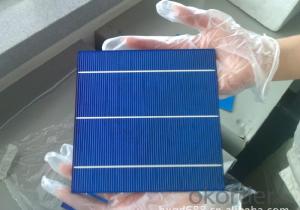
3 Bus Bars 156*156 17.4% efficiency poly solar cell
Dimension: 156 mm x 156 mm ± 0.5 mm
Wafer Thickeness: 156 mm x 156 mm ± 0.5 mm

Typical Electrical Characteristics:
| Efficiency code | 1660 | 1680 | 1700 | 1720 | 1740 | 1760 | 1780 | 1800 | 1820 | 1840 | 1860 |
| Efficiency (%) | 16.6 | 16.8 | 17.0 | 17.2 | 17.4 | 17.6 | 17.8 | 18.0 | 18.2 | 18.4 | 18.6 |
| Pmax (W) | 4.04 | 4.09 | 4.14 | 4.19 | 4.23 | 4.28 | 4.33 | 4.38 | 4.43 | 4.48 | 4.53 |
| Voc (V) | 0.612 | 0.615 | 0.618 | 0.621 | 0.624 | 0.627 | 0.629 | 0.63 | 0.633 | 0.635 | 0.637 |
| Isc (A) | 8.42 | 8.46 | 8.51 | 8.56 | 8.61 | 8.65 | 8.69 | 8.73 | 8.77 | 8.81 | 8.84 |
| Imp (A) | 7.91 | 7.99 | 8.08 | 8.16 | 8.22 | 8.27 | 8.33 | 8.38 | 8.43 | 8.48 | 8.53 |
* Testing conditions: 1000 W/m2, AM 1.5, 25 °C, Tolerance: Efficiency ± 0.2% abs., Pmpp ±1.5% rel.
* Imin : at 0.5 V
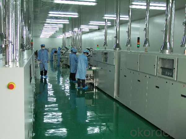
Production:

Package:

FAQ:
1. Q: Do you have your own factory?
A: Yes, we have. Our factory located in Jiangsu
2. Q: How can I visit your factory?
A: Before you visit,please contact us.We will show you the route or arrange a car to pick you up.
3. Q: Do you provide free sample?
A: Commenly we provide paid sample.
4. Q: Could you print our company LOGO on the nameplate and package?
A: Yes, we accept it.And need an Authorization Letter from you.
5. Q: Do you accept custom design on size?
A: Yes, if the size is reasonable.
6. Q: How can I be your agent in my country?
A: Please leave feedback. It's better for us to talk about details by email.
7. Q: Do you have solar project engineer who can guide me to install system?
A: Yes, we have a professional engineer team. They can teach you how to install a solar system.
- Q: How is the bandgap of a solar silicon wafer determined?
- The bandgap of a solar silicon wafer is determined through various experimental techniques, such as photoluminescence spectroscopy or optical absorption measurements. These methods involve shining light of different wavelengths onto the wafer and measuring the corresponding response, which helps determine the energy difference between the valence and conduction bands, known as the bandgap.
- Q: Can solar silicon wafers be used in other applications besides solar energy?
- Yes, solar silicon wafers can be used in other applications besides solar energy. They are commonly used in the production of semiconductor devices and integrated circuits. These wafers serve as a crucial component in various electronic devices, such as computer chips, microprocessors, and sensors. Additionally, solar silicon wafers can be utilized in the manufacturing of photovoltaic systems for applications like solar-powered calculators and portable chargers.
- Q: In the silicon surface cleaning, there is a final step, the silicon chip into the 4% concentration of HF solution soak for five minutes, to hydrogen passivation treatment, and then rinse with deionized water after nitrogen drying,What is the role and mechanism of this hydrogen passivation?
- 0.5 ~ 1min in order to achieve the effect of removing the damage layer, at this timeCorrosion rate can reach 6 to 10um/min.In the polishing process to remove the damage layer on the basis to try to reduce, to prevent corrosion of the wafer was too thin.
- Q: How are solar silicon wafers protected from vandalism?
- Solar silicon wafers are typically protected from vandalism through various measures, including the installation of security fences and surveillance systems around the solar panel arrays. Additionally, some solar farms employ security personnel to monitor the premises and deter potential vandals. The use of anti-climbing devices, such as barbed wire or spikes, is also common to prevent unauthorized access to the panels. Overall, a combination of physical barriers, technology, and human intervention helps safeguard solar silicon wafers from vandalism.
- Q: What is the thickness of the semiconductor wafer used today?I have consulted some for solar wafers, heard now that the wafer thickness in 200~400 micron, but we need the wafer thickness requirements for high now, that for semiconductor wafer thickness is slightly higher than the solar energy, but I do not know how much is there in about 1 mm
- 0.670mm or so. The wafer must be thinned, otherwise the loss of the dicing knife is very large, and it is necessary to draw two knives
- Q: Can solar silicon wafers be damaged by hail or other weather conditions?
- Yes, solar silicon wafers can be damaged by hail or other severe weather conditions. Hailstones can cause physical impact damage, leading to cracks or fractures on the wafers. Additionally, extreme weather conditions like heavy storms, high winds, or lightning strikes can also pose risks to the integrity of solar panels, including the silicon wafers. It is essential to consider the potential impact of weather conditions and take appropriate measures to protect solar panels from potential damage.
- Q: How do solar silicon wafers perform in polluted environments?
- Solar silicon wafers are generally designed to withstand various environmental conditions, including pollution. However, the performance of solar silicon wafers in polluted environments can be affected to some extent. Pollutants such as dust, smog, or particulate matter can accumulate on the surface of the wafers, reducing their ability to absorb sunlight effectively. This can result in a decrease in the overall efficiency of the solar panels. Regular cleaning and maintenance of the wafers can help mitigate the impact of pollution and ensure optimal performance.
- Q: Can solar silicon wafers be used in other applications besides solar panels?
- Yes, solar silicon wafers can be used in various other applications besides solar panels. They are commonly used in electronics, such as integrated circuits and microchips, due to their excellent electrical conductivity and thermal properties. Additionally, they can be utilized in the production of sensors, optoelectronics, and even in certain medical devices. The versatility and reliability of solar silicon wafers make them suitable for a range of applications beyond solar panels.
- Q: How thick are solar silicon wafers?
- Solar silicon wafers typically have a thickness ranging from 150 to 200 micrometers (μm), which is about 0.15 to 0.2 millimeters (mm).
- Q: Can solar silicon wafers be used in solar-powered security systems?
- Yes, solar silicon wafers can be used in solar-powered security systems. These wafers are commonly used in the production of solar cells, which convert sunlight into electricity. By harnessing solar energy, security systems can operate independently, without relying on grid power or batteries. Solar silicon wafers provide a reliable and sustainable solution for powering security systems, ensuring continuous surveillance even in remote or off-grid locations.
Send your message to us
Solar Panel Silicon Wafer - High Current 16.6% Polycrystalline Silicon Solar Cell
- Ref Price:
-
- Loading Port:
- Shanghai
- Payment Terms:
- TT OR LC
- Min Order Qty:
- 1000 pc
- Supply Capability:
- 100000 pc/month
OKorder Service Pledge
OKorder Financial Service
Similar products


Hot products


Hot Searches
Related keywords

