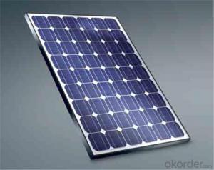
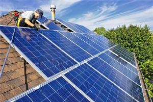
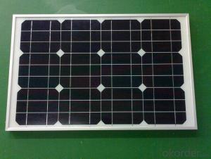


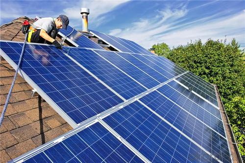
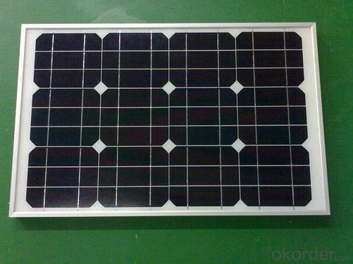


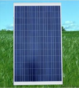
240w Mono Silicon Solar Wafer Panels for Home Use Solar Power System
- Ref Price:
-

- Loading Port:
- China main port
- Payment Terms:
- TT OR LC
- Min Order Qty:
- 10000 watt
- Supply Capability:
- 20000000 watt/month
OKorder Service Pledge
OKorder Financial Service
You Might Also Like


Destription:
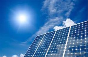
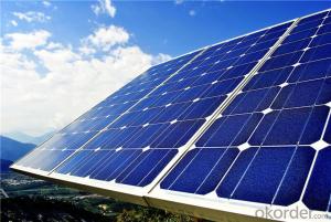
Solar panel refers to a panel designed to absorb the sun's rays as a source of energy for generating electricity or heating. A PV module is a packaged, connected assembly of typically 6×10 solar cells. Solar PV panels constitute the solar array of a photovoltaic system that generates and supplies solar electricity in commercial and residential applications.
Main Characteristic
1.Manufactured according to international quality and Environment Management
System (ISO9001, ISO14001)
2. By the high transmittance, low iron tempered glass, anti-aging of the EVA(polyethylene - vinyl acetate), high-performance crystalline silicon solar cells, good Weather resistance TPT (fluoroplastics composite membrane) by pyramid , has a good Weather resistance and anti-UV, hail, water-proof capacity.
3. OEM and customerized package are accepted
4. High efficiency crystalline silicon solar cells
Quality warranty
1.10 years limited warranty on material and workmanship
2. more than 90% power output in 10 years
3. more than 80% power output in 25 years
Product show


- Q: Why is it not easy to use high resistance on the silicon chip integrated circuit
- In some places, the resistance of the epitaxial layer is adopted, and the resistance is N type, which has a lot of inconvenience in the circuit, and the numerical value is also very difficult to do
- Q: How are solar silicon wafers protected from transportation damage?
- Solar silicon wafers are typically protected from transportation damage through various measures, such as packaging them in special containers or boxes that provide cushioning and shock absorption. These containers often include foam inserts or other materials that prevent the wafers from moving or vibrating during transit, minimizing the risk of breakage or cracking. Additionally, some manufacturers may use specialized handling procedures and equipment to ensure safe transportation of the wafers, reducing the potential for damage during loading, unloading, or movement.
- Q: It is said that monocrystalline silicon, polycrystalline silicon wafer cutting requirements and problems are still quite a lot of
- 3, with line (intensive line): because the grinding ability of mortar mortar or not slicing machine loop system, caused by the silicon dense line region.4, because the hydraulic cutting machine: dislocation line clamping device surface residual glue mortar and other foreign matter or pallet, causing the hydraulic device and the plate can not be completely clamped, and plate screw loosening, resulting.
- Q: Are there any advancements in solar silicon wafer manufacturing techniques?
- Yes, there have been significant advancements in solar silicon wafer manufacturing techniques. Researchers and industry professionals have been actively working on improving the efficiency, cost-effectiveness, and scalability of silicon wafer production for solar cells. Some of the advancements include the development of new slicing technologies, such as diamond wire sawing, which enables thinner and more precise wafer cutting. Additionally, there have been innovations in wafer cleaning and surface texturing techniques to enhance light absorption and reduce reflection losses. Furthermore, the use of kerfless wafering techniques and advanced doping processes are being explored to optimize the material utilization and improve cell performance. Overall, these advancements aim to make solar silicon wafer manufacturing more efficient, sustainable, and capable of meeting the increasing demand for clean energy.
- Q: How do solar silicon wafers handle shading or partial obstruction?
- Solar silicon wafers are generally designed to handle shading or partial obstruction quite well. While shading can reduce the overall energy output of a solar panel, modern panels are equipped with bypass diodes that allow electricity to flow around the shaded or obstructed cells, ensuring continuous power generation. Additionally, advanced panel designs and installation techniques help minimize the impact of shading, such as using microinverters or power optimizers that maximize the energy harvest from each individual cell. Overall, solar silicon wafers are engineered to withstand partial shading and obstruction, ensuring efficient energy production even under suboptimal conditions.
- Q: How is the surface of a solar silicon wafer treated?
- The surface of a solar silicon wafer is treated through a combination of cleaning and texturization processes. Initially, the wafer is cleaned to remove any impurities or contaminants. This is typically done using a combination of chemical and mechanical cleaning methods. After cleaning, the surface is texturized to increase its light absorption capability. One common method is to etch the surface using a mixture of chemicals, creating a rough texture. This textured surface helps to trap and scatter light, enhancing the efficiency of the solar cell. Once treated, the surface is typically coated with a thin layer of anti-reflective material to further improve light absorption. The treated wafer is then ready to be used in the fabrication of solar cells.
- Q: What is the reason for the original or the original silicon?
- The complaint can be suppliers, with hydrofluoric acid washed off after processed velvet
- Q: How is a busbar created in a solar silicon wafer?
- A busbar in a solar silicon wafer is created by using a conductive material, typically silver paste or aluminum, that is screen-printed onto the wafer's surface. This material is then fired at high temperatures to create a durable and efficient electrical connection for collecting and transmitting the electricity generated by the solar cells.
- Q: How is the back surface field created in a solar silicon wafer?
- The back surface field in a solar silicon wafer is created through a process called diffusion. In this process, a dopant impurity is diffused into the back surface of the wafer, creating a layer with an opposite charge carrier type compared to the rest of the wafer. This creates a built-in electric field at the back surface, which helps in reducing recombination of charge carriers and improving the overall efficiency of the solar cell.
- Q: What are the main challenges in the production of solar silicon wafers?
- One of the main challenges in the production of solar silicon wafers is the high energy consumption involved in the manufacturing process. The production of silicon wafers requires a significant amount of energy, particularly during the purification and crystallization stages. This poses a challenge in terms of the environmental impact and the overall sustainability of the process. Another challenge is the high cost associated with producing high-quality silicon wafers. The fabrication process requires precise control over various parameters such as temperature, pressure, and impurity levels, which can be expensive to maintain. Additionally, the raw materials used in the production, such as high-purity silicon, are costly, further adding to the overall production expenses. Furthermore, ensuring consistent and uniform quality across all produced wafers is another challenge. Variations in thickness, impurity levels, and crystal structure can have a significant impact on the efficiency and performance of solar cells. Thus, maintaining strict quality control measures throughout the production process is crucial but can be technically demanding and time-consuming. Lastly, the production of silicon wafers also generates a considerable amount of waste, including silicon dust and other byproducts. Proper disposal and recycling of these waste materials pose a challenge in terms of environmental sustainability and efficient resource management. Overall, addressing these challenges in energy consumption, cost, quality control, and waste management is essential to enhance the efficiency and sustainability of solar silicon wafer production.
Send your message to us
240w Mono Silicon Solar Wafer Panels for Home Use Solar Power System
- Ref Price:
-
- Loading Port:
- China main port
- Payment Terms:
- TT OR LC
- Min Order Qty:
- 10000 watt
- Supply Capability:
- 20000000 watt/month
OKorder Service Pledge
OKorder Financial Service
Similar products
Hot products


Hot Searches
Related keywords

