

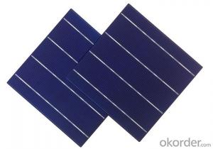

Crystalline Silicon Wafer Solar Cells - A Grade Polycrystalline Solar Cell 4.2W-4.3W
- Ref Price:
-

- Loading Port:
- China main port
- Payment Terms:
- TT OR LC
- Min Order Qty:
- 100 watt
- Supply Capability:
- 10000 watt/month
OKorder Service Pledge
OKorder Financial Service
You Might Also Like


A Grade Polycrystalline Solar Cell 4.2W-4.3W
Main Characteristic
17.6%-18% High Efficiency A Grade 125mm Monocrystalline Solar Cells
1.First-class production technology and packaging technology.
2.Adopting the world's leading technology of silicon and polycrystalline silicon cells, power density, peak hours more battery power, higher conversion efficiency.
3.Beautiful, stable, easy to take down the anodic aluminum frame electric degrees and has a wind-resistant, anti-snow function.
Features
17.6%-18% High Efficiency A Grade 125mm Monocrystalline Solar Cells
1.High transmissivity low-iron tempered glass, strong aluminium frame.
2.Manufactured according to international quality and Environment Management System (ISO9001, ISO14001).
3.Low voltage-temperature coefficient allows higher power output at high-temperature condition.
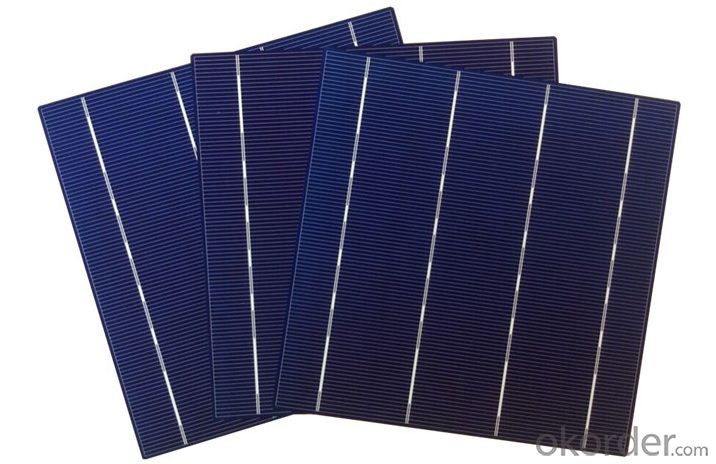
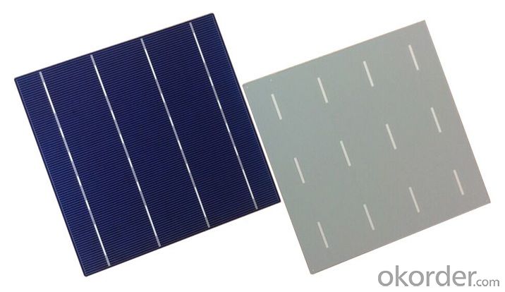
Product Pictures


Top 7 Reasons to Order From Us:
1) We offer you the best quality on the market!
2) We offer you strongly competitive prices !
3) We offer the fastest shipping !
4) we can accept small order!
5) we design various of watt according to cuatomer!
6) We have the best customer service team!
7) We have excellent manufacturer solar panel warranty policy!
- Q: Can solar silicon wafers be used in solar-powered water pumps?
- Yes, solar silicon wafers can be used in solar-powered water pumps. The wafers are used to convert sunlight into electricity, which can then be used to power the water pump.
- Q: What are the properties of a high-quality solar silicon wafer?
- A high-quality solar silicon wafer possesses several key properties. Firstly, it should have a high level of purity, typically exceeding 99.9999%, to ensure minimal impurities and defects. Additionally, it should exhibit excellent crystallographic orientation and uniformity to enhance the efficiency of solar cells. The wafer's thickness and surface quality are also crucial factors, requiring precise control and minimal imperfections to optimize light absorption and electron movement. Furthermore, a high-quality wafer should have low electrical resistance, allowing efficient charge carrier transport. Lastly, it should possess a low rate of light-induced degradation to ensure long-term stability and performance.
- Q: How is the surface of a solar silicon wafer textured?
- The surface of a solar silicon wafer is textured by using various techniques such as acid etching or laser ablation. These methods create a pattern of tiny pyramidal or needle-like structures on the surface, which helps to trap and scatter light, increasing the absorption efficiency of the silicon wafer.
- Q: What is the cost of a solar silicon wafer?
- The cost of a solar silicon wafer can vary depending on several factors such as the size, quality, and quantity being purchased. On average, a standard 156 mm x 156 mm solar silicon wafer can range from $0.10 to $0.30 per piece. However, prices may fluctuate due to market conditions and supplier negotiations.
- Q: What is a silicon wafer cutting edge material?
- Online cutting process, the cutting fluid (usually polyethylene glycol) and cutting edge material sand spray with the fall in thin steel wire by thin steel wire net, high speed, make the mortar in cutting edge material and pressed online silicon rod or a silicon ingot surface high speed grinding,
- Q: Are solar silicon wafers affected by power grid fluctuations?
- No, solar silicon wafers are not directly affected by power grid fluctuations. Solar panels generate electricity independently of the power grid, using sunlight to produce energy. However, fluctuations in the power grid can indirectly impact the overall efficiency and performance of solar panels, as they rely on a stable grid connection for grid-tied systems or for energy storage purposes.
- Q: Are all solar panels made with silicon wafers?
- No, not all solar panels are made with silicon wafers. While silicon is the most commonly used material for solar panels, there are also other types of solar panels available such as thin-film solar panels that utilize different materials like cadmium telluride or copper indium gallium selenide.
- Q: Can solar silicon wafers be used in solar-powered drones?
- Yes, solar silicon wafers can be used in solar-powered drones. Solar silicon wafers are commonly used to convert sunlight into electricity, making them an ideal choice for powering drones with solar energy.
- Q: What is the expected growth rate for the solar silicon wafer market?
- The expected growth rate for the solar silicon wafer market is projected to be significant, with estimates ranging from 6% to 8% annually.
- Q: How does the crystal structure of a solar silicon wafer affect its performance?
- The crystal structure of a solar silicon wafer plays a crucial role in determining its performance. The wafer's crystal structure affects its electrical properties, such as conductivity and efficiency, which directly impact the efficiency of solar cells made from these wafers. A well-aligned crystal structure with minimal defects allows for better electron flow and reduces recombination losses, resulting in higher conversion efficiency. Additionally, a uniform crystal structure ensures consistent performance across the entire wafer, maximizing the overall energy output of the solar cell.
Send your message to us
Crystalline Silicon Wafer Solar Cells - A Grade Polycrystalline Solar Cell 4.2W-4.3W
- Ref Price:
-
- Loading Port:
- China main port
- Payment Terms:
- TT OR LC
- Min Order Qty:
- 100 watt
- Supply Capability:
- 10000 watt/month
OKorder Service Pledge
OKorder Financial Service
Similar products


Hot products


Hot Searches
Related keywords

