
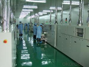


Solar Silicon Wafer Price - High Quality A Grade Polycrystalline 5V 16.0% Solar Cell
- Ref Price:
-

- Loading Port:
- Shanghai
- Payment Terms:
- TT OR LC
- Min Order Qty:
- 1000 pc
- Supply Capability:
- 100000 pc/month
OKorder Service Pledge
OKorder Financial Service
You Might Also Like


Specifications
hot sale solar cell
1.16.8%~18.25% high efficiency
2.100% checked quality
3.ISO9001/ISO14001/TUV/CE/UL
4.stable performance
We can offer you the best quality products and services, don't miss !
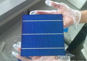
POLY6'(156*156)
Polycrystalline Silicon Solar cell
Physical Characteristics
Dimension: 156mm×156mm±0.5mm
Diagonal: 220mm±0.5mm
Thickness(Si): 200±20 μm
Front(-) Back(+)
Blue anti-reflecting coating (silicon nitride); Aluminum back surface field;
1.5mm wide bus bars; 2.0mm wide soldering pads;
Distance between bus bars: 51mm . Distance between bus bars :51mm .
Electrical Characteristics
Efficiency(%) | 18.00 | 17.80 | 17.60 | 17.40 | 17.20 | 16.80 | 16.60 | 16.40 | 16.20 | 16.00 | 15.80 | 15.60 |
Pmpp(W) | 4.33 | 4.29 | 4.24 | 4.19 | 4.14 | 4.09 | 4.04 | 3.99 | 3.94 | 3.90 | 3.86 | 3.82 |
Umpp(V) | 0.530 | 0.527 | 0.524 | 0.521 | 0.518 | 0.516 | 0.514 | 0.511 | 0.509 | 0.506 | 0.503 | 0.501 |
Impp(A) | 8.159 | 8.126 | 8.081 | 8.035 | 7.990 | 7.938 | 7.876 | 7.813 | 7.754 | 7.698 | 7.642 | 7.586 |
Uoc(V) | 0.633 | 0.631 | 0.628 | 0.625 | 0.623 | 0.620 | 0.618 | 0.617 | 0.615 | 0.613 | 0.611 | 0.609 |
Isc(A) | 8.709 | 8.677 | 8.629 | 8.578 | 8.531 | 8.478 | 8.419 | 8.356 | 8.289 | 8.220 | 8.151 | 8.083 |

MONO5'(125*125mm)165
Monocrystalline silicon solar cell
Physical Characteristics
Dimension: 125mm×125mm±0.5mm
Diagonal: 165mm±0.5mm
Thickness(Si): 200±20 μm
Front(-) Back(+)
Blue anti-reflecting coating(silicon nitride); Aluminum back surface field;
1.6mmwide bus bars; 2.5mm wide soldering pads;
Distance between bus bars: 61mm . Distance between bus bars :61mm .
Electrical Characteristics
Efficiency(%) | 19.40 | 19.20 | 19.00 | 18.80 | 18.60 | 18.40 | 18.20 | 18.00 | 17.80 | 17.60 | 17.40 | 17.20 |
Pmpp(W) | 2.97 | 2.94 | 2.91 | 2.88 | 2.85 | 2.82 | 2.79 | 2.76 | 2.73 | 2.70 | 2.67 | 2.62 |
Umpp(V) | 0.537 | 0.535 | 0.533 | 0.531 | 0.527 | 0.524 | 0.521 | 0.518 | 0.516 | 0.515 | 0.513 | 0.509 |
Impp(A) | 5.531 | 5.495 | 5.460 | 5.424 | 5.408 | 5.382 | 5.355 | 5.328 | 5.291 | 5.243 | 5.195 | 4.147 |
Uoc(V) | 0.637 | 0.637 | 0.636 | 0.635 | 0.633 | 0.630 | 0.629 | 0.629 | 0.628 | 0.626 | 0.626 | 0.625 |
Isc(A) | 5.888 | 5.876 | 5.862 | 5.848 | 5.839 | 5.826 | 5.809 | 5.791 | 5.779 | 5.756 | 5.293 | 5.144 |

FAQ:
Q:How can i get some sample?
A:Yes , if you want order ,sample is not a problem.
Q:How about your solar panel efficency?
A: Our product efficency around 17.25%~18.25%.
Q:What’s the certificate you have got?
A: we have overall product certificate of ISO9001/ISO14001/CE/TUV/UL
- Q: How are solar silicon wafers affected by light-induced degradation?
- Solar silicon wafers are affected by light-induced degradation in terms of reduced efficiency and performance. This degradation occurs due to the formation of defects and impurities in the silicon material when exposed to intense sunlight over time. As a result, the solar cells on these wafers experience a decrease in power output and a decrease in overall conversion efficiency. This degradation can be mitigated through various techniques, such as using higher-quality silicon, implementing anti-reflection coatings, or incorporating passivation layers to minimize the impact of light-induced degradation.
- Q: How do defects affect the efficiency of a solar silicon wafer?
- Defects in a solar silicon wafer can significantly impact its efficiency. These defects, such as impurities or crystal lattice irregularities, can hinder the flow of electrons, leading to reduced conductivity and lower conversion of sunlight into electricity. Moreover, defects can create recombination centers that capture and recombine electron-hole pairs, further decreasing the overall efficiency of the solar cell. Therefore, minimizing defects in the manufacturing process is crucial to ensure optimal performance and maximize the efficiency of a solar silicon wafer.
- Q: How is a mounting structure attached to a solar silicon wafer?
- A mounting structure is typically attached to a solar silicon wafer using a strong adhesive or soldering technique. This attachment ensures the wafer is securely held in place, allowing for proper alignment and stability within the solar panel assembly.
- Q: Mainly want to understand its physical principles and processing technology, thank you
- 1M=1024KB1KB=1024B1B=8b (note, lowercase)The computer is used 1024 of the hexadecimal, real life is commonly used in the, which is why the 512MB card, plug in the computer but only about 488MB
- Q: Can solar silicon wafers be used in tandem with other types of solar cells?
- Yes, solar silicon wafers can be used in tandem with other types of solar cells. Tandem solar cells, also known as multi-junction solar cells, are devices that consist of multiple layers of different types of solar cells stacked together. By combining solar silicon wafers with other types of solar cells, such as thin-film or perovskite cells, it is possible to achieve higher efficiencies and better performance in converting sunlight into electricity.
- Q: Can solar silicon wafers be used in other applications besides solar panels?
- Yes, solar silicon wafers can be used in other applications besides solar panels. They are also commonly used in the production of semiconductors, integrated circuits, and various electronic devices due to their excellent electrical properties and high purity.
- Q: How are solar silicon wafers protected from extreme weather events?
- Solar silicon wafers are typically protected from extreme weather events through the use of encapsulants and protective coatings. These materials shield the wafers from moisture, UV radiation, and temperature fluctuations, ensuring their durability and longevity in various weather conditions. Additionally, solar panels are designed and installed with robust mounting systems to withstand strong winds, storms, and other extreme weather events.
- Q: How is a solar silicon wafer cut?
- A solar silicon wafer is typically cut using a wire saw or a diamond saw. The process involves feeding a wire or a blade made of diamond crystals through the silicon ingot, which is slowly rotated and sliced into thin wafers. This method ensures precision and minimal material loss during the cutting process.
- Q: What is the maximum voltage a solar silicon wafer can handle?
- The maximum voltage a solar silicon wafer can handle depends on various factors such as its thickness, quality, and design. However, typically, most solar silicon wafers can handle a maximum voltage of around 600-1000 volts.
- Q: What is the role of solar silicon wafers in space exploration?
- Solar silicon wafers play a crucial role in space exploration as they are the primary component of solar panels used to generate electricity in space. These wafers are made from highly purified silicon and are capable of converting sunlight into electrical energy, providing a reliable and sustainable power source for space missions. Without solar silicon wafers, it would be challenging to power spacecraft and satellites for long durations in space, limiting our ability to explore and gather valuable data about our universe.
Send your message to us
Solar Silicon Wafer Price - High Quality A Grade Polycrystalline 5V 16.0% Solar Cell
- Ref Price:
-
- Loading Port:
- Shanghai
- Payment Terms:
- TT OR LC
- Min Order Qty:
- 1000 pc
- Supply Capability:
- 100000 pc/month
OKorder Service Pledge
OKorder Financial Service
Similar products


Hot products


Hot Searches
Related keywords

