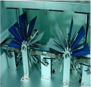
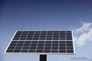
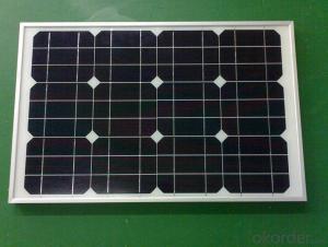
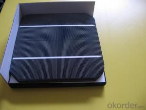
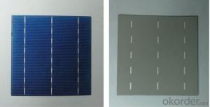
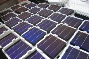
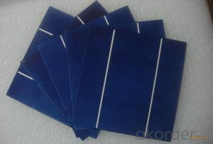
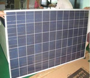
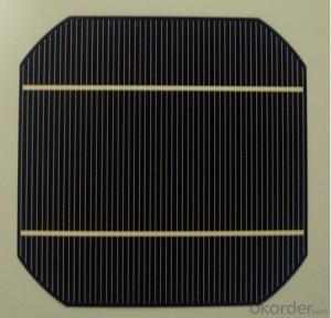
Silicon Wafer for Solar Energy - High Quality A Grade Polycrystalline 5V 16.6% Solar Cell
- Loading Port:
- Shanghai
- Payment Terms:
- TT OR LC
- Min Order Qty:
- 1000 pc
- Supply Capability:
- 100000 pc/month
OKorder Service Pledge
OKorder Financial Service
You Might Also Like
Specifications
hot sale solar cell
1.16.8%~18.25% high efficiency
2.100% checked quality
3.ISO9001/ISO14001/TUV/CE/UL
4.stable performance
We can offer you the best quality products and services, don't miss !
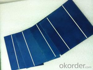
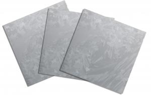
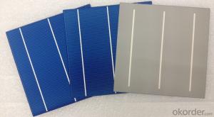
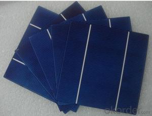
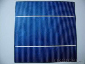
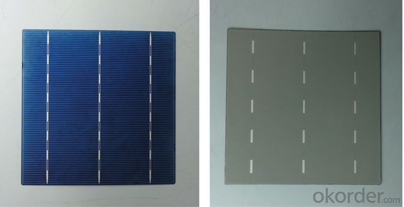
POLY6'(156*156)
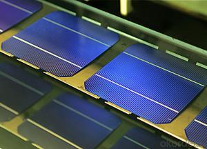
Polycrystalline Silicon Solar cell
Physical Characteristics
Dimension: 156mm×156mm±0.5mm
Diagonal: 220mm±0.5mm
Thickness(Si): 200±20 μm
Front(-) Back(+)
Blue anti-reflecting coating (silicon nitride); Aluminum back surface field;
1.5mm wide bus bars; 2.0mm wide soldering pads;
Distance between bus bars: 51mm . Distance between bus bars :51mm .
Electrical Characteristics
Efficiency(%) | 18.00 | 17.80 | 17.60 | 17.40 | 17.20 | 16.80 | 16.60 | 16.40 | 16.20 | 16.00 | 15.80 | 15.60 |
Pmpp(W) | 4.33 | 4.29 | 4.24 | 4.19 | 4.14 | 4.09 | 4.04 | 3.99 | 3.94 | 3.90 | 3.86 | 3.82 |
Umpp(V) | 0.530 | 0.527 | 0.524 | 0.521 | 0.518 | 0.516 | 0.514 | 0.511 | 0.509 | 0.506 | 0.503 | 0.501 |
Impp(A) | 8.159 | 8.126 | 8.081 | 8.035 | 7.990 | 7.938 | 7.876 | 7.813 | 7.754 | 7.698 | 7.642 | 7.586 |
Uoc(V) | 0.633 | 0.631 | 0.628 | 0.625 | 0.623 | 0.620 | 0.618 | 0.617 | 0.615 | 0.613 | 0.611 | 0.609 |
Isc(A) | 8.709 | 8.677 | 8.629 | 8.578 | 8.531 | 8.478 | 8.419 | 8.356 | 8.289 | 8.220 | 8.151 | 8.083 |
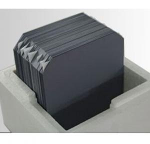
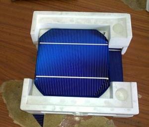
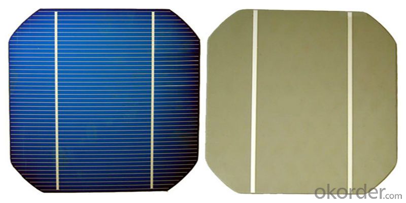
MONO5'(125*125mm)165
Monocrystalline silicon solar cell
Physical Characteristics
Dimension: 125mm×125mm±0.5mm
Diagonal: 165mm±0.5mm
Thickness(Si): 200±20 μm
Front(-) Back(+)
Blue anti-reflecting coating(silicon nitride); Aluminum back surface field;
1.6mmwide bus bars; 2.5mm wide soldering pads;
Distance between bus bars: 61mm . Distance between bus bars :61mm .
Electrical Characteristics
Efficiency(%) | 19.40 | 19.20 | 19.00 | 18.80 | 18.60 | 18.40 | 18.20 | 18.00 | 17.80 | 17.60 | 17.40 | 17.20 |
Pmpp(W) | 2.97 | 2.94 | 2.91 | 2.88 | 2.85 | 2.82 | 2.79 | 2.76 | 2.73 | 2.70 | 2.67 | 2.62 |
Umpp(V) | 0.537 | 0.535 | 0.533 | 0.531 | 0.527 | 0.524 | 0.521 | 0.518 | 0.516 | 0.515 | 0.513 | 0.509 |
Impp(A) | 5.531 | 5.495 | 5.460 | 5.424 | 5.408 | 5.382 | 5.355 | 5.328 | 5.291 | 5.243 | 5.195 | 4.147 |
Uoc(V) | 0.637 | 0.637 | 0.636 | 0.635 | 0.633 | 0.630 | 0.629 | 0.629 | 0.628 | 0.626 | 0.626 | 0.625 |
Isc(A) | 5.888 | 5.876 | 5.862 | 5.848 | 5.839 | 5.826 | 5.809 | 5.791 | 5.779 | 5.756 | 5.293 | 5.144 |
FAQ:
Q:How can i get some sample?
A:Yes , if you want order ,sample is not a problem.
Q:How about your solar panel efficency?
A: Our product efficency around 17.25%~18.25%.
Q:What’s the certificate you have got?
A: we have overall product certificate of ISO9001/ISO14001/CE/TUV/UL
- Q: How are solar silicon wafers protected from electrostatic discharge?
- Solar silicon wafers are protected from electrostatic discharge through a variety of methods. One common approach is to implement antistatic coatings on the surface of the wafer, which help to dissipate any electrostatic charges that may build up. Additionally, during the manufacturing process, these wafers are often handled in controlled environments with proper grounding and the use of ionized air blowers to minimize static electricity. This ensures that the wafers remain protected and do not get damaged by electrostatic discharge.
- Q: What is the role of surface recombination velocity on solar silicon wafers?
- The surface recombination velocity on solar silicon wafers plays a crucial role in determining the efficiency of solar cells. It refers to the rate at which charge carriers (electrons and holes) recombine at the surface of the wafer. A high surface recombination velocity leads to increased recombination, resulting in a loss of generated carriers and reduced cell efficiency. Therefore, minimizing the surface recombination velocity is essential to enhance the performance of solar cells by maximizing carrier collection and reducing energy losses.
- Q: How do solar silicon wafers perform in cold climates?
- Solar silicon wafers perform well in cold climates as the low temperatures actually enhance their efficiency. The cold weather helps to reduce the resistance in the solar cells, allowing them to produce more electricity. However, extreme cold can lead to issues such as snow accumulation, which may temporarily hinder their performance until cleared. Overall, solar silicon wafers are designed to withstand and operate efficiently in cold weather conditions.
- Q: What is the role of a solar silicon wafer in solar energy generation?
- The role of a solar silicon wafer in solar energy generation is to serve as the main component of a solar cell. These wafers are made from highly purified silicon and are responsible for converting sunlight into electricity through the photovoltaic effect. The wafer acts as a platform for other layers and materials to be added, such as metal contacts and anti-reflective coatings, to enhance the efficiency of the solar cell. Ultimately, the solar silicon wafer plays a crucial role in capturing and converting solar energy into usable electricity.
- Q: How are solar silicon wafers affected by potential-induced degradation?
- Solar silicon wafers are negatively affected by potential-induced degradation (PID). PID occurs when high voltage potential differences between the solar cells and their grounded frames cause leakage currents to flow through the silicon wafers. This leads to a decrease in the power output and efficiency of the solar panels over time. PID can significantly impact the performance and lifespan of solar photovoltaic systems, making it crucial to implement preventive measures and use PID-resistant materials and designs to mitigate its effects.
- Q: Can solar silicon wafers be damaged by hail or other weather conditions?
- Yes, solar silicon wafers can be damaged by hail or other severe weather conditions. Hailstones can cause physical impact damage, cracking or shattering the wafers, which can affect the efficiency and functionality of solar panels. Additionally, extreme weather conditions like high winds, heavy rain, or lightning strikes can also potentially cause damage to the silicon wafers. Proper installation and protective measures can help mitigate these risks.
- Q: What are the main challenges in manufacturing solar silicon wafers?
- One of the main challenges in manufacturing solar silicon wafers is achieving high purity levels of the silicon material. Impurities can hinder the efficiency of solar cells, so extensive purification processes are required to remove impurities. Another challenge is the high energy consumption involved in the manufacturing process. It takes a significant amount of energy to produce the high temperatures needed to melt and refine the silicon. Finding ways to reduce energy consumption and increase process efficiency is a constant challenge. Additionally, the production of silicon wafers involves a complex and delicate process that requires precise control and handling. Maintaining consistent thickness, quality, and uniformity throughout the wafer is crucial for optimal solar cell performance. Lastly, the cost of manufacturing solar silicon wafers remains a challenge. Developing cost-effective manufacturing techniques and scaling up production to meet the increasing demand for solar energy are ongoing challenges in the industry.
- Q: How does the thickness of a passivation layer affect the efficiency of a solar silicon wafer?
- The thickness of a passivation layer significantly affects the efficiency of a solar silicon wafer. A thicker passivation layer creates a stronger barrier between the silicon wafer and the surrounding environment, reducing surface recombination and enhancing charge carrier lifetime. This results in higher overall efficiency of the solar cell as it allows for more effective utilization of the incident sunlight. However, there is an optimal thickness range for the passivation layer, as an excessively thick layer can introduce additional surface defects, leading to decreased efficiency.
- Q: What are the advantages of using solar silicon wafers?
- There are several advantages of using solar silicon wafers. Firstly, they have excellent light absorption properties, allowing them to efficiently convert sunlight into electricity. Secondly, they are durable and have a long lifespan, with many solar panels lasting over 25 years. Additionally, silicon is abundantly available and relatively inexpensive, making it a cost-effective option for solar energy production. Furthermore, silicon wafers can be easily manufactured at large scales, making them suitable for mass production of solar panels. Lastly, solar silicon wafers are environmentally friendly as they produce clean energy, reducing carbon emissions and dependence on fossil fuels.
- Q: Can solar silicon wafers be used in solar-powered gadgets?
- Yes, solar silicon wafers can be used in solar-powered gadgets. Silicon wafers are the main component in solar cells, which convert sunlight into electricity. These solar cells can be integrated into various solar-powered gadgets, such as solar panels, solar chargers, and solar-powered lights.
Send your message to us
Silicon Wafer for Solar Energy - High Quality A Grade Polycrystalline 5V 16.6% Solar Cell
- Loading Port:
- Shanghai
- Payment Terms:
- TT OR LC
- Min Order Qty:
- 1000 pc
- Supply Capability:
- 100000 pc/month
OKorder Service Pledge
OKorder Financial Service
Similar products
Hot products
Hot Searches
Related keywords
