

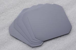


Solar Silicon Wafer - Monocrystalline Grade
- Ref Price:
-

- Loading Port:
- Shanghai Port
- Payment Terms:
- TT or LC
- Min Order Qty:
- 100Pieces PCS
- Supply Capability:
- 700 MW/Per Year PCS/month
OKorder Service Pledge
OKorder Financial Service
You Might Also Like


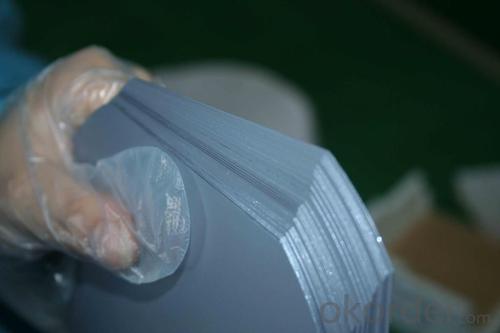
Specification of Mono Silicon Wafers
We can provide you solar wafer both156*156 and 125*125mm, Mono and Poly
Solar Wafers for your raw materials choice.
| Product name | Mono Wafer |
| Conductive type | P type |
| Square size wafer(mm) | 156×156±0.5 |
| Resistivity range | 1~3 ohm |
| Corner(mm) | 150±0.5;165±0.5 |
| 195±0.5;200±0.5 | |
| Thickness (μm) | 200±20 |
| Total thickness(um) | ≤ 30 |
| Resistivity range(Ωcm) | 1-3 |
| Doping elements | Boron |
| Orientation | (100)±1° |
| Carbon content(atoms/cc) | ≤1.0E+17 |
| Oxygen content(atoms/cc) | ≤1.0E+18 |
| Lifetime(μs) | ≥10 |
| Surface quality | No crack, gap, missing Angle, perforated, silicon fell and stress |
| Warping degrees(warp/μm) | ≤50 |
| Neighbouring vertical degree | 90±0.5° |
| Side damage(mm) | ≤0.5mm(length)×0.3mm(width)(not more than 2 per wafer) |
| Line mark(μm) | ≤15 |
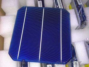
Usage and Applications of Mono Solar Wafers
Mono Solar Wafers mainly used in Solar Cells with reliable quality and trustful efficiency performance. Our Wafers should be your best choice for raw materials.
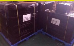
Packaging & Delivery of Mono Solar Wafers
Carton Box Package and Deliver by air. It should be avoid of moist, water and shaking to protect the safety of Solar Cells.
Factory Picture of Mono Solar Wafers

Package Picture of Mono Solar Wafers

- Q: What is the role of antireflection coatings on solar silicon wafers?
- The role of antireflection coatings on solar silicon wafers is to reduce the amount of light reflection and increase the amount of light absorption by the solar cells. These coatings are designed to minimize the loss of incident light at the surface of the silicon wafer, allowing more sunlight to penetrate the material and be converted into electricity. By reducing reflection, antireflection coatings enhance the overall efficiency and performance of solar panels.
- Q: Can solar silicon wafers be used in recreational vehicles (RVs)?
- Yes, solar silicon wafers can be used in recreational vehicles (RVs) to generate electricity from sunlight and power various appliances and systems within the vehicle.
- Q: Is the thickness of solar cell silicon wafer certain? Specifically how much
- The rest is just the substrate, it doesn't work. Do not understand, then you can look at the film thickness of the battery, you will understand.
- Q: Why should the wafer cut side, cut out edge Jiaosha
- In fact, early silicon is not cutting edge, but with the development of microelectronics industry began the following reasons: cutting edge, W2) i: J n$W% L* M1 s `&;1, n can do a plurality of microelectronic devices on the wafer, cut down, and there is a crystal to crystal growth requirements, cutting along a direction for cutting chaos crack, cleavage is the professional said. The cutting edge tells you the direction of cleavage.2, N type and P type silicon wafer, a standard trimming is also inform you that it is n type or P type electrical characteristics, electrical characteristics, u$J2 z/ h 9 - O3, microelectronics production has been automated, such as lithography exposure if there is no cutting edge positioning, then the mask plate and the chip will be a difference of 180 degrees or a certain location, production efficiency will be very low...,4, the use of a lot of silicon, in addition to n/p also have crystal direction, for example, do MEMS requires corrosion anisotropy will be used <110> crystal direction, and MOS products in order to reduce the influence of the surface state requirements with <100> crystal...
- Q: How do solar silicon wafers perform in polluted urban areas?
- Solar silicon wafers perform relatively well in polluted urban areas, as they are designed to withstand various environmental conditions. However, the efficiency of solar panels may be slightly reduced due to the presence of air pollutants, such as dust particles or smog, which can partially obstruct sunlight. Regular cleaning and maintenance are recommended to ensure optimal performance and to mitigate any potential impact from pollution.
- Q: Are there any government regulations or standards for solar silicon wafers?
- Yes, there are government regulations and standards for solar silicon wafers. These regulations and standards are put in place by various governmental bodies to ensure the quality, efficiency, and safety of solar silicon wafers used in the production of solar panels. These regulations may include specifications on the purity, dimensions, chemical composition, and electrical properties of silicon wafers. Compliance with these regulations and standards is necessary for manufacturers to maintain industry standards and meet the requirements for government incentives or certifications.
- Q: How are solar silicon wafers protected against corrosion?
- Solar silicon wafers are protected against corrosion through the use of passivation techniques. These techniques involve applying a thin layer of protective material, such as silicon nitride or silicon oxide, to the surface of the wafers. This protective layer acts as a barrier, preventing the silicon underneath from coming into contact with moisture or other corrosive elements in the environment. Additionally, the wafers are often encapsulated within a protective module, such as a glass or polymer sheet, which further shields them from corrosion.
- Q: How do solar silicon wafers perform in low light conditions?
- Solar silicon wafers perform relatively well in low light conditions compared to other solar technologies. Although their efficiency decreases, they can still generate electricity due to their ability to convert even small amounts of sunlight into energy. However, their performance is significantly reduced during overcast skies or in shaded areas where access to direct sunlight is limited.
- Q: What is the effect of power output on the performance of a solar silicon wafer?
- The power output of a solar silicon wafer directly impacts its performance. Higher power output indicates that the wafer can generate more electricity, leading to increased efficiency and effectiveness in converting sunlight into usable energy. A higher power output allows for greater electricity generation and better overall performance of the solar silicon wafer.
- Q: How do solar silicon wafers perform in high-pollution environments?
- Solar silicon wafers are designed to withstand high-pollution environments quite well. The protective coatings on the surface of the wafers help to prevent dirt, dust, and other pollutants from adhering to the surface. Additionally, the rugged construction of the wafers ensures they can handle harsh weather conditions and prolonged exposure to pollutants without significant degradation in performance. However, it is still recommended to regularly clean the solar panels in high-pollution areas to maintain their optimal efficiency.
1. Manufacturer Overview
| Location | |
| Year Established | |
| Annual Output Value | |
| Main Markets | |
| Company Certifications |
2. Manufacturer Certificates
| a) Certification Name | |
| Range | |
| Reference | |
| Validity Period |
3. Manufacturer Capability
| a) Trade Capacity | |
| Nearest Port | |
| Export Percentage | |
| No.of Employees in Trade Department | |
| Language Spoken: | |
| b) Factory Information | |
| Factory Size: | |
| No. of Production Lines | |
| Contract Manufacturing | |
| Product Price Range | |
Send your message to us
Solar Silicon Wafer - Monocrystalline Grade
- Ref Price:
-
- Loading Port:
- Shanghai Port
- Payment Terms:
- TT or LC
- Min Order Qty:
- 100Pieces PCS
- Supply Capability:
- 700 MW/Per Year PCS/month
OKorder Service Pledge
OKorder Financial Service
Similar products


Hot products


Hot Searches
Related keywords

