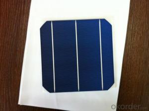
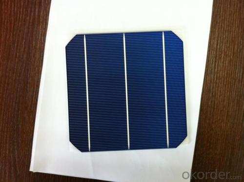
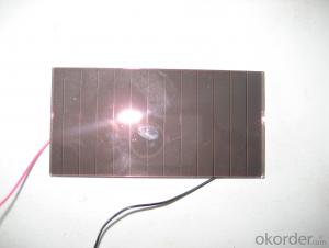
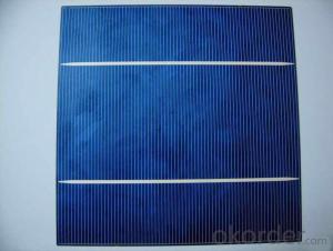
Silicon Wafer Solar Cell - High Quality A Grade Mono Crystalline 5V 17.2%
- Loading Port:
- Shanghai
- Payment Terms:
- TT OR LC
- Min Order Qty:
- 1000 pc
- Supply Capability:
- 100000 pc/month
OKorder Service Pledge
OKorder Financial Service
You Might Also Like
Specifications
hot sale solar cell
1.16.8%~18.25% high efficiency
2.100% checked quality
3.ISO9001/ISO14001/TUV/CE/UL
4.stable performance
We can offer you the best quality products and services, don't miss !
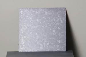
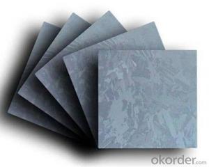
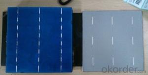
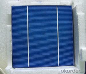
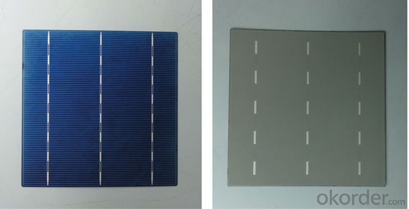
POLY6'(156*156)
Polycrystalline Silicon Solar cell
Physical Characteristics
Dimension: 156mm×156mm±0.5mm
Diagonal: 220mm±0.5mm
Thickness(Si): 200±20 μm
Front(-) Back(+)
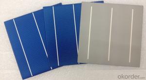
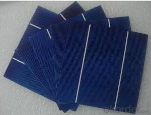
Blue anti-reflecting coating (silicon nitride); Aluminum back surface field;
1.5mm wide bus bars; 2.0mm wide soldering pads;
Distance between bus bars: 51mm . Distance between bus bars :51mm .
Electrical Characteristics
Efficiency(%) | 18.00 | 17.80 | 17.60 | 17.40 | 17.20 | 16.80 | 16.60 | 16.40 | 16.20 | 16.00 | 15.80 | 15.60 |
Pmpp(W) | 4.33 | 4.29 | 4.24 | 4.19 | 4.14 | 4.09 | 4.04 | 3.99 | 3.94 | 3.90 | 3.86 | 3.82 |
Umpp(V) | 0.530 | 0.527 | 0.524 | 0.521 | 0.518 | 0.516 | 0.514 | 0.511 | 0.509 | 0.506 | 0.503 | 0.501 |
Impp(A) | 8.159 | 8.126 | 8.081 | 8.035 | 7.990 | 7.938 | 7.876 | 7.813 | 7.754 | 7.698 | 7.642 | 7.586 |
Uoc(V) | 0.633 | 0.631 | 0.628 | 0.625 | 0.623 | 0.620 | 0.618 | 0.617 | 0.615 | 0.613 | 0.611 | 0.609 |
Isc(A) | 8.709 | 8.677 | 8.629 | 8.578 | 8.531 | 8.478 | 8.419 | 8.356 | 8.289 | 8.220 | 8.151 | 8.083 |
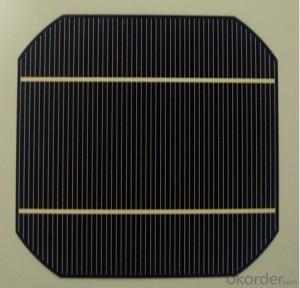
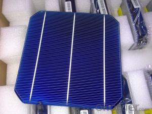
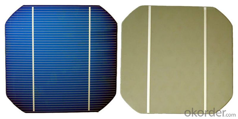
MONO5'(125*125mm)165
Monocrystalline silicon solar cell
Physical Characteristics
Dimension: 125mm×125mm±0.5mm
Diagonal: 165mm±0.5mm
Thickness(Si): 200±20 μm
Front(-) Back(+)
Blue anti-reflecting coating(silicon nitride); Aluminum back surface field;
1.6mmwide bus bars; 2.5mm wide soldering pads;
Distance between bus bars: 61mm . Distance between bus bars :61mm .
Electrical Characteristics
Efficiency(%) | 19.40 | 19.20 | 19.00 | 18.80 | 18.60 | 18.40 | 18.20 | 18.00 | 17.80 | 17.60 | 17.40 | 17.20 |
Pmpp(W) | 2.97 | 2.94 | 2.91 | 2.88 | 2.85 | 2.82 | 2.79 | 2.76 | 2.73 | 2.70 | 2.67 | 2.62 |
Umpp(V) | 0.537 | 0.535 | 0.533 | 0.531 | 0.527 | 0.524 | 0.521 | 0.518 | 0.516 | 0.515 | 0.513 | 0.509 |
Impp(A) | 5.531 | 5.495 | 5.460 | 5.424 | 5.408 | 5.382 | 5.355 | 5.328 | 5.291 | 5.243 | 5.195 | 4.147 |
Uoc(V) | 0.637 | 0.637 | 0.636 | 0.635 | 0.633 | 0.630 | 0.629 | 0.629 | 0.628 | 0.626 | 0.626 | 0.625 |
Isc(A) | 5.888 | 5.876 | 5.862 | 5.848 | 5.839 | 5.826 | 5.809 | 5.791 | 5.779 | 5.756 | 5.293 | 5.144 |
FAQ:
Q:How can i get some sample?
A:Yes , if you want order ,sample is not a problem.
Q:How about your solar panel efficency?
A: Our product efficency around 17.25%~18.25%.
Q:What’s the certificate you have got?
A: we have overall product certificate of ISO9001/ISO14001/CE/TUV/UL
- Q: Can solar silicon wafers be used in smart grid applications?
- Yes, solar silicon wafers can be used in smart grid applications. Smart grids require efficient and sustainable energy sources, and solar silicon wafers are a key component of solar panels, which are a popular renewable energy solution. By harnessing solar power, these wafers can contribute to the generation of clean electricity for smart grid systems, enabling better energy management, distribution, and integration with advanced technologies.
- Q: How do solar silicon wafers contribute to reducing carbon emissions?
- Solar silicon wafers contribute to reducing carbon emissions by enabling the production of solar panels, which generate clean and renewable electricity from sunlight. As the main component of solar cells, silicon wafers capture sunlight and convert it into electrical energy without emitting greenhouse gases or pollutants. By replacing fossil fuel-based energy sources, solar silicon wafers help reduce reliance on carbon-intensive electricity generation, ultimately mitigating carbon emissions and combating climate change.
- Q: What is the role of surface recombination on solar silicon wafers?
- The role of surface recombination on solar silicon wafers is to reduce the efficiency of the solar cells. Surface recombination refers to the loss of charge carriers (electrons and holes) at the surface of the silicon wafer, which can significantly limit the performance of the solar cells. By reducing the surface recombination, the efficiency of the solar cells can be improved, leading to higher power output and better overall performance of the photovoltaic system.
- Q: What is the effect of doping on the bandgap of a solar silicon wafer?
- Doping in a solar silicon wafer has a significant effect on its bandgap. By selectively adding impurities to the silicon lattice, the bandgap of the material can be modified. Doping with elements such as phosphorus or boron can either increase or decrease the bandgap of silicon. N-type doping, which involves adding phosphorus, introduces extra electrons into the lattice, reducing the bandgap. This allows the material to absorb photons with lower energies, extending the wavelength range of solar absorption. P-type doping, using boron, creates "holes" in the lattice, increasing the bandgap. This enables the material to absorb photons with higher energies, expanding its efficiency in converting sunlight into electricity. Overall, doping plays a crucial role in tailoring the bandgap of solar silicon wafers to optimize their performance in photovoltaic applications.
- Q: How do defects affect the efficiency of a solar silicon wafer?
- Defects in a solar silicon wafer can significantly affect its efficiency. These defects, such as impurities or structural abnormalities, can reduce the overall performance of the solar cell by hindering the flow of electrons or creating recombination centers. This leads to a decrease in the conversion of sunlight into electricity, resulting in a lower energy output. Therefore, minimizing defects is crucial for ensuring optimal efficiency in solar silicon wafers.
- Q: Can solar silicon wafers be used in electric vehicle charging stations?
- Yes, solar silicon wafers can be used in electric vehicle charging stations. They can be utilized to capture sunlight and convert it into electricity, which can then be used to power the charging stations, providing a sustainable and renewable source of energy for electric vehicles.
- Q: Can solar silicon wafers be used in military or defense applications?
- Yes, solar silicon wafers can be used in military or defense applications. They can be integrated into various defense systems and equipment, such as unmanned aerial vehicles (UAVs), surveillance systems, and portable power solutions for soldiers in the field. Solar silicon wafers provide a reliable and sustainable source of energy, making them suitable for military operations in remote or off-grid locations.
- Q: Are all solar silicon wafers the same color?
- No, solar silicon wafers can come in different colors depending on the manufacturing process and the specific materials used.
- Q: How is an interconnect created in a solar silicon wafer?
- An interconnect in a solar silicon wafer is created by using a combination of processes such as metallization, screen printing, and firing. Metallization involves depositing a thin layer of metal, typically silver, on the surface of the wafer to create a conductive pathway. Screen printing is then used to apply a paste made of metal particles onto the metallized areas, forming the interconnect lines. Finally, the wafer is subjected to a high-temperature firing process, which helps to fuse the metal particles and create a strong electrical connection between the interconnect lines and the underlying solar cells.
- Q: What is the effect of surface roughness on solar silicon wafers?
- The effect of surface roughness on solar silicon wafers is twofold. Firstly, it can enhance light trapping, increasing the absorption of sunlight and consequently improving the efficiency of the solar cells. Secondly, excessive surface roughness can lead to increased recombination of charge carriers, reducing the overall performance of the solar cells. Therefore, achieving an optimal level of surface roughness is crucial for maximizing the efficiency of solar silicon wafers.
Send your message to us
Silicon Wafer Solar Cell - High Quality A Grade Mono Crystalline 5V 17.2%
- Loading Port:
- Shanghai
- Payment Terms:
- TT OR LC
- Min Order Qty:
- 1000 pc
- Supply Capability:
- 100000 pc/month
OKorder Service Pledge
OKorder Financial Service
Similar products
Hot products
Hot Searches
Related keywords
