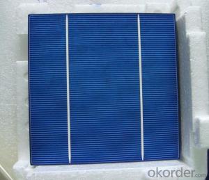
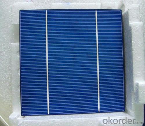


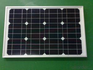
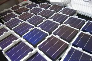
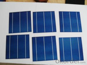
A Silicon Wafer Solar Cell - High Current 18.2% Polycrystalline Silicon Solar Cell
- Ref Price:
-

- Loading Port:
- Shanghai
- Payment Terms:
- TT OR LC
- Min Order Qty:
- 1000 pc
- Supply Capability:
- 100000 pc/month
OKorder Service Pledge
OKorder Financial Service
You Might Also Like


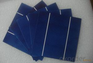
4 Bus Bars 156*156 17.6% efficiency poly solar cell
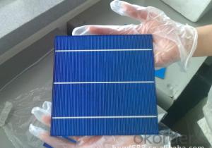
PHYSICAL CHARACTERISTICS
Dimension: 156mm x 156mm ± 0.5mm
Wafer Thickeness: 180um+20um and 200um+20um
Front(-) Four 1.2mm silver busbar
Silicon nitride blue anti-reflection coating
Back(+) aluminum back surface field
1.75mm(silver) wide segment soldering pads

Typical Electrical Characteristics
Efficiency | W(Pmpp) | V(Umpp) | A(Impp) | V(Uoc) | A(Isc) |
17.4-17.5 | 4.234 | 0.517 | 8.231 | 0.622 | 8.759 |
17.5-17.6 | 4.259 | 0.519 | 8.243 | 0.623 | 8.769 |
17.7-17.8 | 4.283 | 0.521 | 8.256 | 0.625 | 8.779 |
17.8-17.9 | 4.307 | 0.523 | 8.268 | 0.626 | 8.788 |
17.9-18.0 | 4.332 | 0.525 | 8.281 | 0.627 | 8.798 |
18.0-18.1 | 4.380 | 0.529 | 8.306 | 0.629 | 8.808 |
18.1-18.2 | 4.405 | 0.531 | 8.318 | 0.632 | 8.818 |
18.2-18.3 | 4.429 | 0.533 | 8.331 | 0.633 | 8.837 |
18.3-18.4 | 4.453 | 0.535 | 8.344 | 0.634 | 8.847 |
18.4-18.5 | 4.478 | 0.537 | 8.356 | 0.636 | 8.856 |
18.5-18.6 | 4.502 | 0.539 | 8.369 | 0.637 | 8.866 |
Efficiency | W(Pmpp) | V(Umpp) | A(Impp) | V(Uoc) | A(Isc) |
20.90-21.00 | 5.06 | 0.557 | 9.007 | 0.653 | 9.688 |
20.80-20.90 | 5.04 | 0.556 | 9.062 | 0.652 | 9.683 |
20.70-20.80 | 5.02 | 0.554 | 9.055 | 0.651 | 9.684 |
20.60-20.70 | 4.99 | 0.552 | 9.033 | 0.651 | 9.672 |
20.50-20.60 | 4.97 | 0.550 | 9.002 | 0.650 | 9.673 |
20.40-20.50 | 4.94 | 0.548 | 9.012 | 0.649 | 9.674 |
20.30-20.40 | 4.92 | 0.546 | 9.009 | 0.649 | 9.655 |
20.20-20.30 | 4.89 | 0.543 | 9.012 | 0.648 | 9.634 |
20.10-20.20 | 4.87 | 0.541 | 8.998 | 0.648 | 9.617 |
20.00-20.10 | 4.85 | 0.540 | 8.977 | 0.647 | 9.600 |
*Data under standard testing conditional (STC):1,000w/m2,AM1.5, 25°C , Pmax:Positive power tolerance.
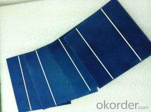
3 Bus Bars 156*156 17.4% efficiency poly solar cell
Dimension: 156 mm x 156 mm ± 0.5 mm
Wafer Thickeness: 156 mm x 156 mm ± 0.5 mm

Typical Electrical Characteristics:
| Efficiency code | 1660 | 1680 | 1700 | 1720 | 1740 | 1760 | 1780 | 1800 | 1820 | 1840 | 1860 |
| Efficiency (%) | 16.6 | 16.8 | 17.0 | 17.2 | 17.4 | 17.6 | 17.8 | 18.0 | 18.2 | 18.4 | 18.6 |
| Pmax (W) | 4.04 | 4.09 | 4.14 | 4.19 | 4.23 | 4.28 | 4.33 | 4.38 | 4.43 | 4.48 | 4.53 |
| Voc (V) | 0.612 | 0.615 | 0.618 | 0.621 | 0.624 | 0.627 | 0.629 | 0.63 | 0.633 | 0.635 | 0.637 |
| Isc (A) | 8.42 | 8.46 | 8.51 | 8.56 | 8.61 | 8.65 | 8.69 | 8.73 | 8.77 | 8.81 | 8.84 |
| Imp (A) | 7.91 | 7.99 | 8.08 | 8.16 | 8.22 | 8.27 | 8.33 | 8.38 | 8.43 | 8.48 | 8.53 |
* Testing conditions: 1000 W/m2, AM 1.5, 25 °C, Tolerance: Efficiency ± 0.2% abs., Pmpp ±1.5% rel.
* Imin : at 0.5 V
Production:

Package:

FAQ:
1. Q: Do you have your own factory?
A: Yes, we have. Our factory located in Jiangsu
2. Q: How can I visit your factory?
A: Before you visit,please contact us.We will show you the route or arrange a car to pick you up.
3. Q: Do you provide free sample?
A: Commenly we provide paid sample.
4. Q: Could you print our company LOGO on the nameplate and package?
A: Yes, we accept it.And need an Authorization Letter from you.
5. Q: Do you accept custom design on size?
A: Yes, if the size is reasonable.
6. Q: How can I be your agent in my country?
A: Please leave feedback. It's better for us to talk about details by email.
7. Q: Do you have solar project engineer who can guide me to install system?
A: Yes, we have a professional engineer team. They can teach you how to install a solar system.
- Q: How are solar silicon wafers protected from bird droppings?
- Solar silicon wafers are typically protected from bird droppings through the installation of anti-reflective coatings on the surface, which make it difficult for bird droppings to adhere to the wafers. Additionally, regular cleaning and maintenance of solar panels can help prevent the accumulation of bird droppings, ensuring optimal performance and efficiency of the solar cells.
- Q: Wafer cutting will appear thick sheet, I would like to ask what the reasons are
- There is a gap between the guide bar and C. silicon block, cut after the start, with the steel wire operation, part of the guide bar is broken into wire, steel wire dislocation, because the steel line will instantly locate in the cutting process, thus causing the phenomenon of silicon chip thickness.D. guide groove wear serious. Guide for coating of polyurethane materials, cutting knife must guide groove root wear, wheel groove cutting process of cutting steel wire side, in the wheel groove due to sloshing around the lead sheet thickness.
- Q: Ask a question about integrated circuit manufacturing: how to realize the functions of capacitors, resistors and transistors on a single chip? In the end how to
- You can look at the aspects of the integrated circuit manufacturing process, integrated circuit design belongs to the back end of these of course, this is not considered in the field of integrated circuit design
- Q: How to make monocrystalline silicon solar panels? Begged: specific steps
- Surface fleeceThe preparation of single crystal silicon wafer is the use of anisotropic etching of silicon on the surface of the silicon per square centimeter to form several million square pyramidal structure, namely, the Pyramid structure. Due to the multiple reflection and refraction of incident light on the surface, the absorption of light is increased, and the short circuit current and conversion efficiency are improved. Anisotropic etching of silicon in alkaline solution liquid is usually hot, available alkali sodium hydroxide, potassium hydroxide, lithium hydroxide and ethylenediamine etc.. Most of them were prepared by using dilute sodium hydroxide solution with a concentration of about 1%, and the corrosion temperature was 70-85. In order to obtain a uniform texture, but also in the solution add alcohols such as ethanol and isopropanol as complexing agent to accelerate the corrosion of silicon. In the preparation of velvet, the silicon chip must be first surface corrosion, alkaline or acidic etching solution to about 20 ~ 25 m, corrosion in the face, the general chemical cleaning. After surface preparation of silicon wafers are not suitable for long-term storage in the water, in order to prevent contamination, should be spread as soon as possible.
- Q: What is the typical cost per watt for a solar silicon wafer?
- The typical cost per watt for a solar silicon wafer ranges from $0.20 to $0.40.
- Q: Are there any advancements in solar silicon wafer manufacturing techniques?
- Yes, there have been significant advancements in solar silicon wafer manufacturing techniques. These advancements aim to improve the efficiency and reduce the cost of solar panel production. Some notable advancements include the use of thinner wafers, such as monocrystalline and polycrystalline silicon wafers, which allow for better light absorption. Additionally, new manufacturing processes like diamond wire sawing and black silicon texturing have been adopted to enhance the efficiency of wafer production. Overall, these advancements contribute to the continuous development of solar technology and its increasing adoption worldwide.
- Q: Can solar silicon wafers be used in remote or inaccessible areas?
- Yes, solar silicon wafers can be used in remote or inaccessible areas. Solar panels made from silicon wafers are highly versatile and can be installed in various locations, even those that are remote or difficult to access. The panels can be transported and installed in these areas to harness solar energy effectively, providing a sustainable and reliable source of power.
- Q: What is the effect of surface passivation on solar silicon wafers?
- Surface passivation on solar silicon wafers helps to reduce the recombination of charge carriers, improving the overall efficiency and performance of solar cells. This process creates a protective layer on the surface of the wafer, minimizing surface defects and preventing the loss of electrons and holes. This enhanced passivation leads to a higher open-circuit voltage, increased fill factor, and ultimately, a higher power conversion efficiency in solar cells.
- Q: How are solar silicon wafers handled during installation?
- During installation, solar silicon wafers are carefully handled to ensure their safety and efficiency. They are typically packaged and transported in protective trays or boxes to prevent any damage or contamination. During the installation process, technicians use specialized tools and equipment to handle the wafers with care, minimizing any physical contact that could potentially harm or scratch their delicate surfaces. Additionally, safety protocols are followed to avoid exposure to dust, moisture, or other harmful elements that could negatively impact the wafers' performance.
- Q: Below what the photovoltaic industry specific industry classification, solar silicon manufacturing enterprises, mainly engaged in single and polycrystalline silicon, polycrystalline silicon wafer cutting casting, single enterprise, what are the concrete classification, a solar silicon slice of this industry?
- Polysilicon for chemical, silicon wafer for machining, battery components for semiconductor processing
Send your message to us
A Silicon Wafer Solar Cell - High Current 18.2% Polycrystalline Silicon Solar Cell
- Ref Price:
-
- Loading Port:
- Shanghai
- Payment Terms:
- TT OR LC
- Min Order Qty:
- 1000 pc
- Supply Capability:
- 100000 pc/month
OKorder Service Pledge
OKorder Financial Service
Similar products


Hot products


Hot Searches
Related keywords

